Quantcast
Channel: Synth Hacker
Viewing all 82 articles
Browse latest View live

Polysix - Sharing my Arduino Code

$
0
0
As many of you know, I made some pretty substantial modifications to my Korg Polysix.  One of the biggest changes was to replace the keybed to enable aftertouch.  To make this happen, I had to replace the Polysix's Key Assigner with an Arduino.  It was a lot of work, but once I made the core hardware modifications, I found that I was able to add lots of features to the Polysix, such as: aftertouch and portamento, more interesting detuning for unison mode, a poly-unison mode, a Moog-like single-trigger mode, and a sustain pedal.  All of these modifications were effected through software changes on the Arduino.

Since I have made those modifications, I have had some people ask if I could share the software.  At first I declined, because I was embarrassed of the poor quality of the code.  I also didn't really know how to share it.  Then, I learned how to use GitHub.  So, I at least know how to share my code now.  All I have to do is get over my embarrassment.  Well, here we go...


If you want to look at some nasty code for how to replace the Polysix Key Assigner using an Arduino, you can find my GitHub repository at: https://github.com/chipaudette/ArduinoPolySix.

Yes, my code is tortured and very difficult to follow.  But, that's what happens when you're just learning how to do this stuff.  Sorry.  If I were to re-write it from scratch it would look a lot different...but this is what I have now.  Maybe you'll find something useful.

Thanks for reading!

Assembling my MCP4922 DAC Breakout

$
0
0
One of my most popular posts was this one on making a simple PCB for the MCP4922 DAC.  I'm so glad that people were interested in this!  After a long delay, I have finally decided that it is time to assemble the PCB.  Let's do it!


This post will be mostly pictures showing how I soldered in the parts.  My technique is pretty poor, so don't take this post as guidance on how you *should* do it.  Instead, take this post as comfort that you can be bad at soldering and still get things to work just fine.

First, I got my MCP4922 chip from Digikey.  Currently, $3.14 each, when bought singly.


I inserted the chip into the PCB.  Fits just fine!


I flipped over the PCB to work on the legs of the chip.


I soldered each of the legs:


With all of the legs are soldered, the picture below shows that the joints in the front row are pretty nice, but that the joints in the back row have too much solder.  Oh well.  I'll try to do better next time.


Upon close inspection, I feel that the legs stick out too far.  So, I trim them with my wire snippers.  I wish I had better snippers.  These don't snip very well.  Better ones might let me snip flush against the PCB.


The chip is now fully soldered in place.  The next step is to add the connectors around the edge of the board.  I could have used male pin headers or female.  I only had male headers on hand, so that's what I used.  As you can see below, I used a blank proto-board to hold the pins in place so that they poke up straight through my PCB.  Then I solder them in place.


Once all the pin headers are in place, I need to solder in the two caps (10 uF and 0.1 uF) to decouple the power supply.  In the design of the PCB, I was bold and made both of them be surface mounted parts.  I have barely worked with surface mount components, so I don't really know what I'm doing.  In the picture below, you see me starting by tinning the pads.  I don't know if this is the right thing to do, but here I go...


After tinning, I try soldering on the surface-mount capacitor.  I'm not sure what the best technique is.  I had to try it several times until I was able to get both ends of the cap to be decently connected.  I am glad that I bought some nice tweezers, though.


So that was the cap on the bottom of the board.  The other cap is on the top of the board.  Unfortunately, I didn't have another surface mount cap of the right value, so I used a small through-hole cap instead.  I snipped the legs really short and tacked it on with solder.  This is not recommended, but it got the job done.


And, finally, I'm finished! (I left one connector unpopulated because that's just an extra connection for power, which I don't need).


With the assembly complete, the next step is to test it.  That'll be the next post!

Testing my MCP4922 PCB

$
0
0
With my custom MCP4922 PCB assembled, it is time to test it.  Soldering is good and fine fun, but the whole point is to get something that actually works!


Connecting to Arduino:  My plan is to connect it to an Arduino and to have it generate a variety of DC voltages.  Unfortunately, it was at this point that I realized I had no female wires to mate to the male headers that I put on my board.  Doh!  So, I had to use alligator clips which are a real pain to work with.  As you can see in the picture above, it is difficult to keep them from touching each other and shorting everything out.

Jumper Some Pins:  Another hiccup is that, as I was hooking it all up to to the Arduino, I realized that I designed my PCB to be overly-general.  Specifically, I when I designed the board, I brought out two of the MCP4922 pins (*SHDN and *LDAC) to the header when I really didn't need to.  For the way that I use this chip, I just need *LDAC tied LOW and *SHDN tied HIGH.  Doing this with alligator clips is annoying, so I just soldered short jumper wires on the bottom of the board to connect these pins to GND and VDD.  This simplified my setup nice.

Arduino Software:  With the hardware all hooked up, I wrote a little Arduino program to drive the DAC.  You can get the code here.  The code outputs two different voltages on the A and B outputs of the DAC to prove that they work.  Output A steps from 0.0V up to 5.0V in one volt increments.  Output B does the opposite -- it steps from 5.0V down to 0.0V in one volt increments.

Victory:  Starting up the program, it automatically stepped through its commands for the different voltages.  I measured the voltages with my digital multi-meter (DMM) to confirm that I was getting the correct output.    As you can see in the pictures below, Output A of the DAC does a pretty good job of hitting the voltages that I wanted.  My first PCB works!  Victory!


Exploring the Error: Because I'm a nerdy guy, I couldn't leave it there.  I couldn't just enjoy my victory in peace.  No.  I had to look at the results in more detail.  Specifically, I was troubled by the fact that the values reported by the DMM were not quite as close to my desired values as I hoped.

Should be Better?:  I hoped to see exact round numbers spanning 0.0 up to 5.0V.  As you can see in the pictures above, my DMM is reporting values that are off by 1-15 mV.  That seems like a lot of error for a 12-bit DAC.  I mean, on the surface, one might expect an accuracy from the DAC of approximately 1 least significant bit (LSB).  One can compute the magnitude of 1 LSB by scaling from the "full scale" voltage of the device.  Since I'm running it at 5.0V, 1 LSB is (5.0 V / 2^12 bits) = (5.0 / 4096) = 1.2 mV.  This is quite a bit smaller than the 15 mV of error that I'm seeing in some cases.  My gut feeling is that I should be doing better.  So, I started to dig into the details...

Error in Full Scale:  First, note that my DMM shows that the "5.0V" case is actually indicating 5.015V.  This suggests that my "full scale" is actually bigger than 5.0V -- that it is actualy 5.015 V.  In my setup, "full scale" is set by the voltage of the power being delivered to the PCB, which is coming from the Arduino.  The Arduino (Uno) is nominally outputs 5.0V, but it is not a precision voltage reference.  For example, the on-board regulator is only good to +/-50 mV and others have also seen their Arduino "5.0V" be off by 12-14 mV.  So I do not find it surprising that full scale voltage could be running 15 mV higher than expected.  If you want a precise "full scale", you probably have to build/buy a precision voltage reference instead of using the Arduino's 5V pin.

New Expected Values:  What does the 5.015V "full scale" value mean for my expectations for the DAC output?  Well,  since all of the DAC's output values are scaled from this full scale value, the output values that I should actually expect to see are 0.000V, 1.003V, 2.006V, 3.009V, 4.012V, and 5.015V.  These values are closer to the ones that I actually saw, which is good.  My measured values are now only off by 0-6 mV (the worst error is for the 2 V reading).  Still, 6 mV is larger than the 1.2 mV error that I might expect based on 1 LSB, so I'm still not satisfied.

DAC Error from Datasheet:  My next idea is that maybe my expectation of 1 LSB accuracy is wrong.  Digging into the datasheet for the MCP4922, I see in the big table on page 5 under "DC Accuracy" that the INL error can be +/- 4 LSB (!).  If 1 LSB is 1.2 mV, then a 4 LSB error would correspond to 4.8 mV.  That's a lot closer to the 6 mV error that I seem to have...but it's still doesn't account for all of it.

Error in DMM:  My next idea is that maybe the error isn't all with the DAC.  Maybe some of the error is in my DMM.  Looking at the user manual for my Extech EX530 digital multi-meter, it states that the device has an accuracy of "+/- (0.06% reading + 2 digits)".  Let's compute what that means for my problematic 2V reading.  First, at 2V, 0.06% is 1.2 mV.  Second, "2 digits" means 2x the value of the smallest digit on the display.  For the 2V reading, the smallest digit is 0.1 mV, so "2 digits" is an error of 0.2 mV.  As a result, the total error for my DMM could be +/- 1.4 mV.

Total Error:  Combining this 1.4 mV of possible error for the DMM with the 4.8 mV of possible error for the DAC, I get a total error of up to 6 mV. This happens to be the same amount of error that I actually saw.  While that's good (I guess), it is also unsatisfying because it requires all of my errors to be at their maximum.  For now, I'm going to accept that.  But, moving forward, I'm going to keep an eye on how closely my DAC's values are to my desired values.

Thanks for reading!

[Note: The comment section of this post is closed due to too much spam from PCB services.]

S-Triggers from TR-707 Drum Machine

$
0
0
I have a Roland TR-707 drum machine and I have a couple of pre-MIDI Korg synths (a Mono/Poly and a Polysix).  Since there's nothing more fun than sweet acid-like basslines combined with propulsive trance-inducing drum beats, it's crucial that my old synths be able to synchronize to the drum machine.  This post is about modifying my 707 to finally make it control my synths the way that they should be controlled -- my 707 now outputs S-Trigs!  First, here's a demo...


Previous Attempts

TR-707 Trigger Out:  The 707 does have an output ("Trigger Out") whose purpose is to synchronize to external gear, such as the arpeggiators in these old synths.  As shown in a previous post, however, the built-in Trigger Out doesn't work for driving the Mono/Poly.  It does work with the Polysix, but it is late by 40 msec due to the V-Trig vs S-Trig issue (as discussed later).  So, in the end, the built-in Trigger Out doesn't work for my old synths.

Arduino MIDI-to-Trigger Converter:  Since the stock 707 Trig Out doesn't work, I hacked together my own MIDI-to-Trigger converter. This Arduino-based device listens to the MIDI clock output by any device (such as from the TR-707) and generates properly synchronized trigger pulses to drive my synths (two arpeggiators at once is fun!).  The problem, though, is that I don't like all the clutter of the extra wiring associated with this setup.  It's not ideal.

Modifying the 707 for S-Trig

V-Trig vs S-Trig:  Why doesn't the 707's built-in Trig Out work?  The problem is that 707 outputs "V-Trig", whereas my old Korgs expect "S-Trig".  What?  A V-Trig is a signal that is normally low (0V), which then pulses high (5V) for each trigger.  Unfortunately, my two old Korg synths expect an "S-Trig", which is the opposite -- a normally high signal that then shorts to ground for each trigger.  This difference between V-Trig and S-Trig means that my 707 doesn't play well with my Korg synths.

The 707 is Actually S-Trig Internally:  After looking through all the schematics, I noticed that inside  the 707, the circuitry actually utilizes S-Trig to trigger its internal drum sounds.  The only V-Trig signal generated by the 707 is the Trig Out provided to the user.  As shown in the schematic excerpt below, even this signal actually starts as an S-Trig that is then inverted into V-Trig by Q13.  So, given that all of these S-Trig signals are already inside the 707, I decided to modify the 707 so that it could output its S-Trig signals.

The TR-707 Trigger Out is "V-Trig", but internally it is "S-Trig"

The Simplest Plan:  Looking at the schematic above, one easy way to output S-Trig would have been to simply take the S-Trig from CPU pin 21 and wire it directly to the output jack.  But, this would have had two problems: (1) these old CPU chips are generally too fragile to be in direct electrical contact with the outside world, and (2) I would have lost the existing V-Trig output, which I might want to use with other gear in the future.  I need a better plan.

A Better Plan:  My better plan is to find a more robust source for S-Trig signals (ie, anything but the CPU) and to output the signal using other jacks on the back of the 707 (so that I keep the built-in Trig Out).  Which jacks?  Well, I never use the cassette tape interface, so I'll re-use those two jacks to give myself *two* S-Trig outputs.  Exciting!

Here's the back of the TR-707.  I'm not going to replace the built-in V-Trig.
Instead, I'll mod the 707 to output S-Trig on these two jacks that I never use.


Re-Wiring the Jacks

Where to Connect:  To use these two jacks, I need to disconnect the jacks from the existing circuit.  Looking at the schematic (excerpt below), the easiest solution would be to remove the resistor R51 for one of the jacks and to remove C30 for the other jack.  While this would work, it's usually a good idea to always have a series resistor in line with an output jack in case someone (ie, me) plugs in something stupid by accident.  The in-line resistor helps limit any currents that could damage the circuitry.  So, to leave a resistor in-line, I chose to pull the right leg of R51 and to pull the right leg of R43.   That disconnects the other circuitry while leaving the resistors in-place for me to re-use later.  It also leaves in-place the capacitor (C30), which I don't want, but which I can deal with later.

I can disconnect the two jacks from the existing circuit by de-soldering the legs of these two resistors.
Smell the Solder:  To disconnect the targeted leg of each resistor, I applied my soldering iron to the back side of the circuit board (PCB) and used small-nosed pliers to wiggle/pull on the resistor leg until it came free.  You can see each resistor's free leg in the photos below.  Later, I'm going to solder a new wire to the free leg, so make sure that the legs are still accessible.

De-soldering one leg of each resistor.  Make sure you de-solder the correct leg!

Getting the S-Trig Signals

Find a Source:  After preparing the output jacks, my next step was to find a good source for S-Trig signals.  Looking at the 707's schematic (see excerpt below), I see that the internal drum sounds are triggered by IC28 (a TC40H174P, which is a basic CMOS flip-flop).  This looks like a great place to get our S-Trig signals because, if IC28 were to get damaged as a result of this mod, this chip is much easier to replace than the CPU itself.  [Note that TC40H174P is no longer available, but a 74LS174 seems to do the same thing].  Let's get our S-Trig signals here.

Get the S-Trig from IC28, because that 40H174 is easy to replace if I damage it.

Soldering in the Wire:  To actually get this signal out, I could solder a wire directly to IC28, but my poor soldering skills mean that I risk damaging the IC by overheating it.  Instead, I'm going to solder my wire to R83, because resistors are very hard to damage.  You can see my soldered result below -- the red wire goes to R83 to get the trigger for the "Rim/Cowbell" sound.  For my second S-Trig, I chose to grab the trigger signal for the "High Tom" (the yellow wire, connecting via R87), but you can choose whichever sound you'd like.

Soldering wires to get the S-Trig signals that I want.

Connecting Back to the Jacks

The Connection Plan:  Now that I have the S-Trig signals on the red and yellow wires, I soldered those wires to the free legs of R51 and R43 (see schematic below).  These are the two resistors that I partially de-soldered from the circuit board to disconnect the jacks from the rest of the circuit.  By soldering to the free leg of each resistor, I've now connected the jacks back to the S-Trig signals produced by IC28.

Connecting the output jacks to the S-Trig signals from R83 and R87.

Jumper C30:  The last modification is to remove the effect of C30 (see schematic above) because it will interfere with the S-Trig signal that I'm trying to output.  The easiest way to "remove" it is to simply solder a jumper wire across its two terminals.  You can see the little jumper that I added in the picture below.  Easy.

I added a jumper wire across C30 to remove it from the circuit.  Otherwise,
it could interfere with outputting the S-Trig signal.

Tuck in the Wires:  The picture below shows my final wiring.  The red wire is connecting the "Rim/Cowbell" trigger from its source on the bottom-right up to the output jack on the top-left.  The yellow wire connects the "High Tom" trigger from the bottom-right up to the top-left.  I tucked in the wires between the components to ease my re-assembly of the drum machine.

The final wiring of the "Rim" and "High Tom" triggers from their source on
bottom-right up to the output jacks on the top-left.

Put It Back Together

With the wiring complete, I re-assembled the drum machine and tested it out.  I confirmed that the built-in "Trig Out" still works (using my Micro Brute, which accepts V-Trig) and I confirmed that my two new S-Trig outputs work (using my Mono/Poly).  You can see my test of the S-Trig outputs in the video at the top.  Hacking success!

I re-used the "Tape Out" and "Tape In" jacks as outputs for S-Trig signals.
The left jack is activated on the "Rim/Cow" triggers.
The right jack is activated on the "High Tom" triggers.


Surface Mount DigiPot with an Arduino Uno

$
0
0
For an upcoming modification to my Korg Polysix, I need to be able to attenuate an analog signal in response to the user's inputs.  This is a perfect task for a a digital potentiometer.  If I can, I'd like to control the digipot from an Arduino, because an Arduino is so easy to program.  There are two challenges with this plan, however.  First, my preferred digipot is only available as a surface mount device.  Second, I'm worried that the Arduino is too slow to drive the digipot quickly.  Well, I do like challenges, so let's just dive in and see where we can get!

Driving my digipot with an Arduino Uno.  How fast can it go?


Choosing my Digipot:  There are many digital potentiometers on the market.  For use inside my Polysix, I might need to put digipot in a place where it would need to control voltages ranging from -5V to +5V.  Most digipots cannot handle this kind of bipolar voltage range (most are just 0-5V).  Of the choices that I saw on Digikey for bipolar digipots, I chose to buy an Analog Devices AD5260 (link).  As you can see it in the picture below, it's a tiny little surface-mount device.  Scary!  (actually, don't be scared...it'll be fine)

Analog Devices AD5260 Digital Potentiometer.  Surface Mount!  Tiny!

Surface-Mount Adapter Board:  Because I'm usually just hacking stuff together, and because through-hole components are much easier to hack with, I don't have nearly zero experience soldering surface-mount components.  If I made my own circuit boards, I would certainly use more surface mount components because they save so much space.  For this hack, however, I need flexibility to plug, unplug, and reconfigure my circuit.  Therefore, I'm going to put my surface mount device onto a an adapter board that gives it legs like a through-hole component.  My digipot is a TSSOP-14 package, so I bought a TSSOP-14 adapter board from Adafruit.  It comes as a pack of 6, so I have spares in case I make a mistake.  :)

Mounting my surface-mount digipot to a through-hole adapter board.

Soldering Surface Mount ICs:  How do I actually do the soldering?  I talked with a co-worker who is extremely experienced in this area and he gave me a pile of good advice.  Two parts of that advice were: (1) use very fine (thin) solder and (2) use lots of flux.  Unfortunately, by the time I got around to soldering (days later), I had forgotten these two important details.  As a result, using my too-thick solder and using no extra flux, I created many solder bridges between the tiny legs of this tiny IC.  This is not what you want to do.  But, through perseverance, and through extensive use of solder wick to remove excess solder, I finally got the IC soldered no shorts or bridges.

Magnification (Or, How to Look Cool):  One piece of my colleague's advice that I did follow was to use some magnification.  He let me borrow an "OptiVisor" (see picture below).  It doesn't feel like it provides much magnification, but it is enough to give a clear view.  And, I'm learning that if you can *see* it, you can solder it.  The OptiVisor provides that.  They're also quite fashionable (that would be sarcasm).  

It definitely helps to use some magnification so that you can see what you're soldering.

Add Legs for Breadboarding:  The Adafruit adapter board has through-holes on either side for attaching pin headers.  As you can see below, I used a regular piece of 0.1" break-away pin header.  I broke off two seven-pin segments, temporarily placed them into my solderless breadboard, put the digipot board on top, and soldered the pins on.  This through-hole stuff is easy!

Soldering the pins to the breakout board so that I can easily prototype with the digipot.
Using a solderless breadboard keeps everything aligned while you solder.

Deciding How to Connect:  With the digipot's adapter board finished, I had to figure out how to wire up the device.  Below is a picture from the digipot's datasheet with my own labels added to show what I would connect to each pin.  All connections were going to my Arduino.  As you can see, there are a bunch of 5V and Gnd connections.  Commands are sent via the SPI bus, so there are also the three SPI connections (theSDO line is not needed as there is no communication needed back to the Arduino).  Finally, for the pot's input, I'll simply apply 5V, which means that my output will be a DC voltage that is scaled between 0-5V.

Signals to use for testing the digipot with an Arduino, which uses 5V logic.

Wiring to the Arduino:  The wiring plan shown above requires 12 connections.  Since I am usually prone to error when doing my wiring, I choose to draw up a little picture to fully illustrate to myself how I should use my solderless breadboard to make all of these connections.  This extra "design" effort really made the wiring process much easier.  It also made the wiring process more reliable.  Once I got the Arduino software working, the wiring of the hardware worked on the first try!

Wiring an Arduino Uno to the my digipot via a solderless breadboard.

Writing the Arduino Software:  To change the value of the digipot, I had to write some Arduino code to send commands to the digipot via the Arduino's SPI pins.  I started with the Arduino's built-in example called "DigitalPotControl".  While that code is simple and easy to understand, I wasn't sure if it runs the SPI bus as the fastest possible setting.  Speed is critical for using this in my Polysix, so this detail was worth a little effort.  After Googling around, I found the correct Arduino commands to control the SPI bus speed and I wrote my test program (SPI mode is zero!).  My program is shared on my GitHub here.

Initial Test:  My test program steps through a range of the digipot values.  It stops at each step for three seconds, which gives me enough time to confirm that its output is correct.  Because the input of my digipot is connected to +5V, my output will be between 0V and 5V.  For the picture below, the digipot was at a value of 125 (out of 255), which resulted in an output voltage being 2.47V.  Given that I expected (125/255*5) = 2.45V, I got pretty decent agreement.  In other words, it works!

First test.  It successfully created a voltage half-way between 0-5V. 

Testing for Speed:  Now for the full speed test.  I commented out the delay() and println() commands and restarted the system.  If used in my Polysix, there will only be 15-20 microseconds (usec) to change value of the digipot.  This means that the Arduino + digipot must support an update rate of 50-67 kHz, which seems pretty fast for an Arduino.  To see how fast my system was actually running, I connected the output of the digipot to an oscilloscope.  The full setup is shown at the picture at the top of this post.  A screenshot from the oscilloscope is shown below.

The Uno is changing the digipot as fast as it can.  It takes 16 usec per step, which results in an update rate of 62.5 kHz.

How Fast is It?  The picture above shows that the digipot is only being updated every 16 usec, which means it has an update rate of 62.5 kHz.  This is within my 50-67 kHz requirement.  So that's good, right?  Well, no, not exactly.  I am a little uncomfortable with the fact that there is no margin.

The Need for Margin:  In achieving this 62.5 kHz result, the Arduino is doing nothing but updating the value of the pot over and over endlessly.  That is all that the Arduino is doing.  In my envisioned hack for Polysix, however, my Arduino would need to do a few other tasks, as well.  For example, the Arduino will need to listen to its Serial port so that it can receive commands as to what values to use for the pot.  If the Arduino is running flat-out just to maintain a high update rate, it probably wouldn't have enough spare cycles to service the serial port.  That would be unacceptable.  So, while it is exciting that I got the system to operate this well, I think that the that the Arduino Uno isn't quite fast enough.  I need to try something else

Trying a Teensy:  My next step is to try a faster Arduino.  Or, an even better plan would be to step up to the fastest Arduino-like board that I know: Teensy 3.  But I think that'll have to wait until my next post.

Update:  My results with the Teensy are here.  The Teensy is *really* fast!

Teensy with AD5260 Digipot

$
0
0
Yesterday, I showed how I soldered a surface-mount digipot, connected it to an Arduino Uno, and got an update rate of just over 60 kHz.  It was pretty fun to get the whole thing working so well.  For my envisioned use of this thing inside my Korg Polsix, however, I need a microcontroller with a little more speed than the Arduino.  It needs to be able to drive the digipot at high speed and do other tasks like listen to messages coming over the serial line.  This post is about using a Teensy to drive the digipot instead.  How fast can it go?

Showing my Teensy 3.1 in the foreground.  It is indeed small.  In the back right is my digipot on its Adafruit SMT-to-DIP adapter board.  An Arduino Uno is in the back left, but it is just being used as a power supply to provide 5V.

What is a Teensy?  Teensy is family of microcontroller boards, like the Arduino is a family of microcontroller boards.  Teensy is aimed at folks who like the Arduino approach but who need something more capable.  In my case, I'm using a Teensy 3.1, which has a 32-bit processor that can run up to 96 MHz.  This is a lot more capability than the 8-bit, 16 MHz processor in the Arduino Uno.  Raw speed, however, isn't my only concern.  The Teensy is appealing to me because you can program it through the Arduino IDE and not have to learn some new way of programming microcontrollers.  Re-using what I know, yet getting more capability.  Sounds like a win-win situation.

Wiring the Digipot for 3.3V Operation:  One somewhat-important difference between an Arduino Uno and a Teensy is that the Teensy operates at 3.3V instead of the Uno's 5V.  This means that the whatever is connected to the Teensy (like my digipot) must be able to respond to the lower voltages.  Lucikly, my digipot is compatible with either 3.3V or 5V logic, so everything should work fine.  The biggest difference is that the output of the digipot (because of the now-smaller 3.3V input signal) will be limited to 0-3.3V, instead of the 0-5V signals seen with the Uno.  For this test, the smaller voltage output is not a problem.  This test is about speed.

Signals to use for testing the digipot with a Teensy 3.1, which uses 3.3V logic.

Wiring to the Teensy:  From the picture above, I'll drive the digipot by providing it power at 3.3V and by sending it commands over via the Teensy's SPI pins.  Looking at the pin map for the Teensy 3.1, I easily see the location of 3.3V and gnd.  Looking for the SPI pins, I see "CS", "SDOUT" and "SCK" on pins 10, 11, and 13, just like on the Arduino Uno!  Maybe that's by design, or maybe it was by coincidence.  Either way, it's comforting to see things being so similar.  So, overall all, as seen below, the wiring is basically the same as it was for the Uno.  Great.

Wiring a Teensy 3.1 to the my digipot via a solderless breadboard.
I connected power (3.3V), ground, and the three lines for the SPI bus.

Teensy Add-On for the Arduino IDE:  With the hardware elements all arranged, it's time to program the Teensy.  Since I want to do this via the Arduino IDE, I needed to first download the "Teensyduino" add-on from the maker of Teensy.  It's pretty painless.  During installation, the installer provides you the option to pre-install a bunch of libraries that Teensy supports.  I chose to install them all, but for this test, you probably just need to install the SPI library.  Either way, it's easy.  Once the Teensyduino software completed its installation, I started the Arduino IDE like normal.  Once it was open, I went under the "Tools" menu (as shown below) and told the Arduino IDE to target the Teensy 3.1 instead of the Arduino Uno.  Done.

I'm switching the Arduino IDE to target my Teensy 3.1 instead of my Arduino Uno.

Programming the Teensy:  With the Teensyduino add-on, my hope was that I could rely on all my Arduino knowledge and not have to learn a new command set just for the Teensy.  Relying on this hope, I simply opened up my existing digipot test program (written for the Arduino Uno) and told the IDE to recompile (Verify" in the language of Arduino).  It was successful!  It recompiled without any changes needed for the Teensy.  Fantastic!  Now, to actually transfer the program down to the Teensy hardware, one has to hit the pushbutton that's on the Teensy board.  When I did that, the program zipped down to the Teensy and I was good to go.  Very smooth.  Very nice.

Driving the Digipot with my Teensy:  With the Teensy programmed and ready-to-go, I hooked up all the wires between my breadboarded digipot and the Teensy according to the figure that I showed earlier.  I then plugged the Teensy into its USB cable (to provide power) and connected my oscilloscope to the output of the digipot.  I saw step-wise changing output voltages, just like I expected.  It worked!

My test setup.  Teensy on the bottom left.  Digipot on a solderless breadboard on the bttom right.  My oscilloscope shows a very quickly changing output signal from the digipot.  It works!

Is it Faster?  How fast could the Teensy change the pot's value?  Very fast.  Very very fast.  As shown in the screenshoot below, it was able to change the value six times in 8.1 microseconds (usec).  That's a mere 1.35 usec per change.  That's an update rate of 741 kHz!  By comparison the Uno required 16 usec, which was an update rate of 62.5 kHz.  So, the Teensy was about 12 times faster for this task.  That's fantastic.  Interestingly, the ratio of the their clock speeds (Teensy = 96 MHz, Uno = 16 MHz) is only 6x, so by actually showing a 12x increase in speed, it appears that the Teensy is much more efficient per clock cycle at this task than the Arduino.  Very cool.

[Note: Based on questions I've received...yes, I did disable the println() and delay() commands when testing at full speed.  I love that you folks are reading in this kind of detail! :) ]

Screenshot of the output of the digipot when being driven at full speed by the Teensy.  Note that it completes a six step cycle in 8.1 usec, which means that each step is only 1.35 usec, which means that the Teensy can drive the digipot with an update rate of 741 kHz.  Fast!

Extra Capacity for Other Tasks:  If I use this Teensy+Digipot setup in my nefarious plans for my Korg Polysix, I do not need it to update this fast.  At worst, I'll need it to update every 20 usec, which means that the Teensy can do its update at its native 1.35 usec speed and then wait around for the other 18.65 usec and do other tasks.  In other words, it'll only be busy (1.35/20) = 7% of the time.  The other 93% of the time, it'll be free to do things like servicing in-coming Serial messages.  I like having that much margin.  It gives me confidence that the Teensy can perform all of its tasks dependably.  My conclusion is that I've found my winning hardware combination for my Polysix modifications.

Velocity Sensitive Polysix - The Dream

$
0
0
As regular readers know, I've done many modifications to my Korg Polysix.  Probably the biggest change was when I swapped out the original keybed for a new one (Fatar, FTW!).  My goal with the new keybed was to add aftertouch to my Polysix, but a side-benefit was that the new keybed was also velocity sensitive.  Unfortunately, the velocity capability has gone unused because the Polysix had no obvious way of including its effect.  Today, though, that begins to change.  Today, I plan out how to add velocity sensitivity to the Polysix.  Behold, the VelocitySix!

Dreaming a Dream of a Dreamy, Velocity-Sensitive, Korg Polysix.  (Fake Graphic)

What Do I Want Velocity to Do?  This is the first question that I asked myself.  What do I want the velocity to affect?  In other synthesizers, the two most traditional answers would be to affect the intensity of the filter (VCF) envelope or of the amplitude (VCA) envelope.  Personally, I've always been a bigger fan of velocity-sensitive VCF, so that's what I decided to target (first, at least).  My idea, therefore, is to add circuitry that will scale the envelope based on the velocity of the keypress.

Scaling the VCF Envelope Based on the Note Velocity

Adding More Hardware:  As can be seen in the figure above, what I need is some hardware that can scale (attenuate) the existing envelope signals.  As discussed in my recent posts, my plan is to do this velocity-dependent attenuation using a digital potentiometer that is driven by a Teensy microcontroller.  I'll simply send the MIDI velocity value for each voice to the Teensy and it will drive the digital potentiometer to adjust the overall amplitude of that voice's VCF envelope.  I'll call the Teensy + digipot my "Velocity Processor".

Piecing it All Together:  The figure below shows all of the components that I've added to my Polysix.  For the addition of velocity sensitivity, I've added my new "Velocity Processor" and highlighted it in yellow.  It is important to realize that I can add this velocity sensitivity only because of my previous modifications.  Without having replaced the built-in keybed with my own keybed and keyscanner, I wouldn't have the velocity values in the first place.  And, without having replaced the built-in "Key Assigner" CPU with my Arduino Mega, I wouldn't know which velocity value to associate with which voice.  It is only through my prior work that this new modification is possible.  [Note: the DAC on the right side of the figure is irrelevant to the velocity sensitivity, but it is crucial for my portamento and detuning modifications.]

My Highly-Modified Polysix.

Building and Testing:  My upcoming posts will discuss the details of how I will manipulate the envelop signals, how I built and tested the new electronics, and how it all sounded when I was done.  This is gonna be fun!


Update:  I've worked out how the Polysix multiplexes its VCF envelopes.

Update:  I've worked out how the Polysix multiplexing handles addressing and synchronization.

Update:  I've wired up the Velocity Processor

Velocity Sensitivity - Understanding the Multiplexing

$
0
0
As discussed in my previous post, I have a dream of adding velocity sensitivity to my Korg Polysix.  My replacement keybed already generates the velocity data, I just have to figure out how to use the data.  My plan is to have the velocity affect the intensity of the envelope applied to the filter (VCF).  The harder I hit the key, the more of the envelope signal is applied to the VCF.  Should be easy, right?  Well, it turns out that the Polysix uses a lot of multiplexing to handle its polyphony, including its VCF control.  This post is about understanding the multiplexing so that I can adjust the envelopes based on note velocity.  Let's go!


The Simplified View:  To figure out how the VCF envelope is applied to the VCF, I looked at the Polysix schematic.  Being a six-voice synth, one might expect that six individual circuits are used to apply six individual envelopes to six individual filters.  But this is not the case.  To save money, the designers used multiplexing so that a single circuit could be used to service all six voices.  When I look at the schematic, I do see that there are six circuits used to create the six envelopes.  But then, at IC24, I see that these six envelope signals are multiplexed into a single time-sliced signal.  The single multiplexed signal is then passed through a circuit that combines the envelopes with the VCF cutoff, the VCF key tracking, and the VCF LFO modulation.  At the end of the circuit, IC23 demultiplexes the time-sliced signal back into six individual control voltages that go off to the filter circuit for each voice.

The Detailed View:  With that overview, I have excerpted the real schematic below and highlighted the signal path specific to the VCF envelope.  As can be seen, the six envelope signals enter at the bottom left.  At IC24, they are multiplexed, at which point the time-sliced envelope signal follows the thin red line through the modulation circuit.  Finally, it ends up back at IC23, were it is demultiplexed back into six control signals for each voice's VCF.  Somewhere in this signal path,  we will make a modification to allow us to modify the VCF envelope based on the note velocity.  To decide where and how to make that modification, I need to better understand how the multiplexing works.

Korg Polysix VCF Envelope Processing Circuit, with Annotations

What Does the Multiplexed Signal Look Like?  I hooked up my oscilloscope to the multiplexed signal line shown in the schematic above.  I hit two keys on the keybed and saw what the multiplexed envelope signal looks like.  In the screenshot below, you can clearly see that two envelopes were triggered.  You can also see that the two envelope signals have been sliced up and interleaved.  This is what multiplexing does, it slices up multiple signals and interleaves them onto a single line.  Looks pretty straight-forward, eh?  Let's zoom in, just to be sure of the details.

Voltage at R58.  Two envelopes are multiplexed onto one line.  The second envelope was triggered 6 msec after the first.

Zoomed View:  The picture below is a zoomed in view of the multiplexed envelopes.  As can be seen, there is a repeating signal that contains two two non-zero voltages.  The first voltage value corresponds to the envelope for Voice #1 at a that specific moment in time.  The second voltage corresponds to the envelope for Voice #4 at its moment in time.  In the time between those two voltages, the voltage is zero because none of the other voices are active.  If the other voices were active (as shown later), there would be signal here.  Since the notes are off, there is no envelope, so there is no signal in that time slot.  Easy.  [As a side note, we see that the mutiplexed signal appears to have a cycle of ~310 microseconds, which means that each voice's envelope gets updated at a rate of 3.2 kHz.  I'm actually a bit surprised that it is that slow.  I expected faster.]

Zoomed in view.  Two envelopes on one line.  The second envelope is the Polysix's voice #4 (out of 6).  Note that the pattern repeats every 310 ms, which means that the envelope for each voice is only updated at 3.2 kHz.

All Six Voices Active:  To further illustrate how the envelopes are multiplexed, the screenshot below shows the multiplexed signal when all six voices are active.  In this case, all of the envelopes were triggered at the same time (Unison mode!) so all of the envelopes are showing approximately the same (non-zero) value.  The critical detail here is that we see six period's worth of non-zero signal.  Those are the six voices.  Curiously, we also see two periods of zero signal.  These extra two slots ("slot 7-8") are, in my opinion, purely an artifact of how the addressing is done to keep the multiplexing and demultiplexing in sync with each other.

View at R58 with all six voices active.  Note the empty space, which implies a voice #7 and #8 (which don't exist).

The Vision for Velocity Sensitivity:  Now that I see how the multiplexing works, I can also see how I can modify the envelope signal based on the velocity of each key press.  I think that I can work directly with the multiplexed signal.  In my illustration below, the left portion of the figure is the multiplexed envelope signal as created by the Polysix.  Each color represents the time slice that is associated with each of the six voices.  My idea is that I can introduce a new circuit -- my "Velocity Processor" -- which can attenuate the envelope signal for each voice, depending upon the velocity of the note assigned to that voice.  As long as my Velocity Processor responds fast enough to keep up with the multiplexing, it can affect each voice independently of the others.


Hardware Configuration:  I like this plan -- to simply modify the multiplexed envelope signal based on each notes velocity.  Looking back at the Polysix's hardware, it looks like the right place to introduce my Velocity Processor would be right after the IC24 Multiplexer, as illustrated in the simplified view below.  This location gives me access to the multiplexed envelope signal, but it is before the signal gets too complicated by the rest of the VCF CV processing, where the cutoff, key tracking, and LFO modulations are applied.


Next Step:  The key to this approach is that I want to independently modify each voice in the multiplexed signal stream.  This means that I need to know which voice is on the multiplexed line at each moment in time.  As a result, I really need to dig in and learn about the synchronization and addressing scheme used by the multiplexer.  Figuring this out will be the topic of my next post.


Velocity Sensitivity - Addressing and Synchronization

$
0
0
In my previous post, I explored how the Polysix multiplexes the VCF envelopes so that one circuit could affect the envelopes for all six different voices.  My goal is to modify each voice' VCF envelope intensity based on the velocity of the note's keypress.  If I am to modify the multiplexed VCF envelope signal based on each voice's velocity, I need to know which voice is on the multiplexed line at each moment in time so that I can apply the correct velocity adjustment for that voice.  The Polysix keeps track of this information via the addressing and synchronization lines used in the multiplexing circuit.  It is these elements that I'm going to explore in today's post.

My plan is to insert my "Velocity Processor" circuitry right after the envelope signals have all been multiplexed by IC24 onto a single line.  The trick is to know which voice is on the multiplexed line at any given moment in time.  This is handled by the synchronization and addressing lines generated by IC12.

Always Look at the Schematic:  When trying to understand the circuit, I always start with the schematic.  Below is an excerpt from the Polysix schematics that show the elements that process the envelopes for the VCF.  The multiplexer is down on the bottom right (IC24) which time-slices all six voices' envelopes to put them onto a single line.  The dark red line is the multiplexed envelope signal.  At the end of the dark red line is the demultiplexer (IC23), which breaks up the multiplexed signal back into the six individual VCF control signals that are sent off ot the six individual voices.  This multiplexing and demultiplexing system only works if the two elements (the multiplexer and demultiplexer) stay in sync.  Synchronization is effected through the addressing line (in blue) and the inhibit lines (in green). It is these signals that I will be looking at.

Korg Polysix VCF Envelope Processing Circuits.  Red line is multiplexed VCF envelope, which then becomes the general VCF CV.  To keep the multiplexer and demultiplexer in sync, the blue lines are the addressing lines and the green lines are the inhibit lines.

Addressing:  If I am to manipulate the multiplexed signal based on the velocity of each note, I need to know which note (which voice) is on the multiplexing line at every moment in time.  The Polysix maintains this information on the blue address lines (A,B,C) that you can see originating from IC12 and that connect to both the multiplexer (IC24) and the demultiplexer (IC25).  The signal on each address line can be either HIGH (5V) or LOW (0V).  Between these three address lines, there are eight different combinations of HIGH and LOW, which means that there are enough combinations to each of the six voices to be associated with one of the eight possible HIGH/LOW combinations.  A particular combination of HIGH/LOW signals, therefore, is an "address" that defines which voice is currently being serviced.

Which Voice For Which Address?  The address signals themselves are generated by IC12, which is a simple binary counter (datasheet).  As a result, you can think of the (A,B,C) address as a 3-bit binary number, where a HIGH voltage corresponds to one for that bit and a LOW voltage corresponds to zero for that bit.  IC12 keeps incrementing that 3-bit number from 1 to 8, over and over, in a never-ending loop.  [Well, actually, it loops over 0 to 7, not 1 to 8, but you get the idea].  As might be expected, the first address points to the first voice, the second address to the second voice, and so on.  Note that the last two addresses are unused -- they exist simply because the dumb binary-counting IC12 is not smart enough to skip address codes that might be unused.


Responding to the Address Lines:  To correctly modulate the multiplexed envelope signal, my Velocity Processor needs to know which voice is being serviced at each moment in time.  Therefore, my Velocity Processor will have to tap into the addressing lines in order to stay synchronized with the mulitplexing.  To interpret those addressing lines, my Velocity Processor must have some sort of "smarts" in order to generate the correct response based on the current address (ie, voice) being indicated.    In other words, my Velocity Processor will have to include a microcontroller that listens to the address lines.

Velocity Processor Configuration:  My Velocity Processor will have two parts -- a microcontroller to respond to the address lines and a digital potentiometer to actually apply the adjustment to the multiplexed envelope signal.  This combination of microcontroller and digipot will be my "Velocity Processor".  As shown in the figure below, I am going to insert my Velocity Processor right after the multiplexer (IC24).  It is a convenient location to get access to both the multiplexed envelope signal and to all of the addressing lines.

Conceptual Design for Attenuating the VCF Envelope Based on a Note's Velocity

How to Change the Multiplexed Signal:  As discussed in the previous post, my plan is to attenuate each voice's VCF envelope based on the voice's note velocity.  The slower the note's velocity, the more attenuation that I am to apply to that voice's envelope.  The digipot is a perfect component to do this function because attenuation is what potentiometers do, and because it is digitally controllable from a microcontroller.  The challenge is for the microcontroller and digipot to keep up with the rapidly-changing multiplexed envelope signal.


How Fast Must The Microcontroller Respond?   If my Velocity Processor is to manipulate the multiplexed signal, it has to to keep up with the multiplexing rate.  More specifically, the multiplexing circuitry includes a "deadband" window of time where it switches between voices -- it is within this deadband that the Velocity Processor must start and finish its task of applying the correct per-voice envelope manipulation.  In the Polysix circuit, this window for action is defined by the INH ("inhibit") signals sent to the multiplexer and demultiplexer.  When the multiplexer and demultiplexer are inhibited, it is our time to act.

Analyzing the INH Signals:  A close look at the schematic shows that there are two INH signals -- one that goes to the multiplexer (IC24), and a different one that goes to the demultiplexer (IC23).  The screenshot below shows these two INH signals over several multiplexing periods.  Whenever the INH signal is HIGH, that's when the output signal is blocked, and that is our time to act.  As can be seen, the multiplexer is inhibited for a short period of time (6-7 microseconds), while the demultiplexer is inhibited for a longer period of time (20 microseconds).  Somewhere in between is the right requirement for my Velocity Processor.

The "Inhibit" Signals Driving the Multiplexer (IC24) and De-Multiplexer (IC23).  These signals define how quickly my new velocity processor circuit must respsond.  It must respond in at most 20 usec, and preferably within 6-7 usec.
It Can Respond Feast Enough:  Lucikly, in a recent post, I showed that my Teensy 3.1 could update my digipot in under 2 microseconds.  Therefore, my Velocity Processor is definitely fast enough.  That's great.

Pulling it All Together:  My plan is to implement a velocity sensitive VCF envelope by manipulating the multiplexed envelope signal.  I found that a set of address and inhibit lines are used by the Polysix to keep the multiplex process synchronized.  If my Velocity Processor is to also be synchronized, it must include a microcontroller that listens to those address lines and responds based on the specific voice being indicated.  I then looked at the timing of the multplex-demultiplex "deadband" window and found that my microcontroller is indeed fast enough to make its changes within that constrained period of time.  As a result, I'm feeling really confident in my approach.

My "Velocity Processor" will be a new element added to my highly-modified Polysix

Building It:  I've already prototyped the digipot + Teensy, so I know that it works and that it is fast enough.  Now I have to figure out how to physically insert it into the Polysix's signal path.  Then, I have to wire it all up, write some software, and start testing.  I'm wicked excited!

Update:  I've built it.  Check it out here!

Building my Polysix Velocity Processor

$
0
0
Today it starts.  We've talked enough about my dreamy dreams of velocity sensitivity for my Korg Polysix.  It's time to get down to business.  It's time to apply what I've learned about its multiplexing and about its synchronization.  It's time to build something.  Let's smell the solder!

First Generation "Velocity Processor" Installed in my Polysix

Where to Insert My Circuity:  Before I solder anything, I need to figure out where I am going to insert my "Velocity Processor" into the Polysix circuit.  As discussed in my previous post, I want to put it after the multiplexer (IC24) but before any of the other envelope and VCF processing.  The figure below shows, notionally, how I'll use several of the signals associated with IC24.  What is the easiest way to get physically access to these signals?


Use the IC24's Socket!  When I opened up my Polysix and too a look at IC24 to see what connection points might be available, I was immediately struck by the fact that IC24 is socketed!  By pulling IC24 out of its socket, I now have instant, easy, and easily-reversible access to most of the signals that I need!

Here is the socket for IC24.  The perfect place for inserting my Velocity Processor.

Which Holes for Which Signals:  Looking at the Polysix schematic, I see that I can get almost all of my signals from this one socket: +5V power and ground, the three addressing lines (A,B,C), the inhibit line (INH) as well as a place to inject my velocity-modified, multiplexed envelope signal.

The signals that I will use for my Velocity Processor -- all available from the socket for IC24.

How to Connect to the Socket:  While the socket is a very convenient way to get signals without modifying the Polysix PCB, I still had to find the right hardware that would mate into the socket.  After trying a few options, I found that the legs on the Arduino-style "stackable" headers fit very nicely into the socket.  My plan, therefore, would be to mount the stackable headers to a protoboard, solder them in place, and have their legs reach down and mate to the socket.  Since these stackable headers have really long legs, they'll let the protoboard (with all of my other components) stand above the other components on the Polysix PCB.  It'll be great!

Arduino-style "stackable" headers fit into the Polysix IC sockets.

Why Not Use Regular 0.1" Pins?  Arduino fans may immediately wonder why I'm using these stackable headers when it appears that 0.1" male pins (also popular with Arduino projects) would be cheaper and less bulky.  In fact, I did try to use these pins.  But they don't fit in the socket.  After looking at the detailed geometry of these pins versus the legs on the stackable header (shown below), I found that the pins are indeed thicker than the legs on the stackable header (0.64 mm vs 0.40 mm).  That's the reason that the pins don't fit.  That's the reason I'm using these stackable headers.  [Note: If you really want to use pins, perhaps the 0.45 mm pins of the Samtech TS-108-T-A will work.]

The common 0.1" male pins are too thick to fit. But pins the stackable female headers are thin enough to work.

General Configuration:  After looking at the space inside the Polysix, and after looking at the size of the protoboard that I had on-hand, I decided to configure the basic elements of my Velocity Processor as shown below.  The stackable headers are shown on the bottom right.  The digipot is on the left.  The Teensy 3.1 microcontroller is on the top.  Now we just need to figure out the wiring.

Here is my high-level plan: a Teensy 3.1 plus a digipot plus a pair of stackable headers.

Connections to the Teensy:  Below is a picture of the Teensy with the pins labeled.  It shows which pins I'm going to use for the various connections.  Remember that the Teensy is only a 3.3V device whereas the Polysix's digital signals (the A,B,C addressing lines and the inhibit line) and the Serial connection from my Arduino key Assigner are all 5V signals.  Luckily the pins on the Teensy 3.1 are 5V tolerant, so I can attach those lines to the Teensy without damaging it.  Another side-effect of the Teensy being 3.3V is that its SPI connections to the digipot will also be 3.3V signals.  Therefore, the digipot will have to be provided with a 3.3V reference, which will come from the wire that I show attached to the Teensy's 3.3V supply.

Connections to my Teensy 3.1

Connections to the Digipot:  Below is a figure showing connections that I'm making to the pins of my digipot.  As mentioned above, the SPI logic signals are at 3.3V, so I connect the "VL" logic reference (pin 12) as well as to the other logic pins.  The multiplexed envelope signal (my "input" to the digipot), however, can span 0V to 5V.  Therefore I set VDD to +5V and VSS to ground.

Connections for the Digipot to handle the 0V-5V Multiplexed Envelope Signal

The Wiring Plan:  The figure below shows my wiring plan for the Teensy, digipot, and IC24 socket.  Of course, I still need IC24 itself to function within the circuit.  Therefore, I had the brilliant idea to insert another IC socket into the stackable headers!  Isn't that brilliant!?!  I happened to have a spare IC socket whose legs seemed just long enough to fit in the big holes of the stackable header.  So, I can build my velocity processor as shown below, insert the board into the vacated socket for IC24, and then stick IC24 into my board.  That's the plan, at least.

The First Wiring Diagram for my Velocity Processor.  Note IC24 sitting on top of the stackable headers in the bottom right.

The Wiring Reality:  Below, you can see the protoboard after I wired and soldered everything in place.  You can even see how I inserted IC24 in place.  On the underside of the board, you can see the pins sticking out that will fit into the Polysix's socket for IC24.

The first version of my Velocity Processor

Testing It:  At the top of this blog post is a picture of this first version of my Velocity Processor mounted within my Polysix.  While it did do something, I quickly discovered that my plan of sticking IC24 on top of the stackable headers wasn't working.  The pins of my add-on IC socket did not mate securely nor reliably to the stackable header.  Sad.

The New Wiring Plan:  The solution to this problem was to move IC24 off the stackable headers and down onto the protoboard.  I had resisted doing this because it mean adding 16 wires (one for each leg of IC24) between the stackable headers and the new spot for IC24.  It was going to be an annoying task, but I needed to do it.  <Sigh>

The Second Wiring Diagram for my Velocity Processor.  Note that IC24 has been moved and 16 additional wires have been added to connect it to the circuit.

The Completed Wiring:  Below is a picture of my Velocity Processor after moving IC24.  You can see it on the top right.  You can also see the rainbow of wires that I had to add to connect IC24 back to the stackable headers.  All those extra wires sure made it ugly.  But, the task is done.

By moving IC24 to its own spot on the top right, the extra wiring really made it ugly.

Plugging It In:  Below is a picture of my revised Velocity Processor mounted within my Polysix.  All of the signals that it needs come up through the IC24 socket into which it has been mounted.  The only exception is the serial communication signal that comes from my Arduino Key Assigner.  That simplicity is pretty nice.

My revised "Velocity Processor" installed in my Polysix. 

Next Steps:   I need to finish the software on the Velocity Processor and I need to write the companion software for the Arduino Key Assigner so that it conveys the velocity data from the keybed to the Teensy.  Then I can test it and make sweet, sweet music.  Stay tuned!

Korg Polysix with Velocity Sensitivity

$
0
0
In truth, a Korg Polysix has rather limited features.  But, because it is an analog synth, it is open to modifications.  And so I've dived in head first.  I've already added aftertouch and portamento, controllable detuning, sustain pedal, and Moog-style legato triggering.  My most recent modifications began a few weeks ago, when I decided that I wanted my Polysix be velocity sensitive.  After a bunch of explorations and trials, I've finally pulled together all of the pieces.  That's today's story.  But first, here's a demo!  (Note, the bass distorts my laptop speakers, too.  Go for headphones.)


The Pieces:  The addition of velocity sensitivity to my Polysix builds upon many of the previous mods that I've done.  The core enabler of this mod was the fact that I had already replaced the stock Polysix keybed (which does not transmit velocity information) with a new Fatar keybed that is both velocity and aftertouch sensitive.  It's sweet.  As shown below, in my modified Polysix, the data from the new keybed is fed to an Arduino Mega, which assigns each new note to one of the six voices in the Polysix.  To modulate that voice in response to the note's velocity, I also feed the velocity information to my new "Velocity Processor", which then does the actual velocity-based modulation.

My highly-modified Polysix.  The newly-added "Velocity Processor" is highlighted in yellow.

Velocity-Based Modulation:  So what kind of velocity sensitivity did I implement?  I chose to modulate the intensity of the filter envelope.  As you heard in the demo, the intensity of the filter opening and closing gives a strong sense of articulation and dynamics.  In a stock Polysix, the intensity is the same for all voices (as set by the "EG Int" knob).  My goal was to dynamically change the envelope intensity based on how hard I hit the key.  As shown below, I chose to attenuate the filter envelope based on the note velocity.  At maximum velocity (MIDI 127), the envelope would be at its full intensity (as set by the "EG Int" knob, as before).  At lower velocity values, the intensity would be progressively smaller.  As a result, notes that I press hard should have a strong intensity and notes that I press lightly will soft intensity.


Scaling the VCF Envelope Based on the Note Velocity

Hardware Approach: After studying the Polysix schematic, and after figuring out how the VCF envelope multiplexing and how its associated addressing and synchronization works, I settled on the plan that I would manipulate the VCF envelopes in the multiplexed portion of its circuit.  Being multiplexed, I only have one signal line to manipulate, instead of six individual signals (one for each voice).  Sure, the signal on that one multiplexed line is changing very quickly (all six envelopes are time-sliced onto a single line), but I've already proved that a Teensy 3.1 plus a digital potentiometer can keep up just fine.  So, my hardware plan was settled -- I'd insert my Velcoity Processor right after the VCF Multiplexer (IC24) on the Polysix's KLM-366 PCB.


Building It:  In the Polysix, I was happy to see that IC24 is socketed, which means that you can pull out the chip and insert all sorts of fun new circuitry via the now-empty socket.  And so that's exactly what I did.  I took a piece of protoboard, soldered on the Teensy 3.1, the digipot, and IC24 itself.  More details on the build are here.  I then inserted the assembled protoboard into the empty IC24 socket.  As you can see below, it's not too pretty.  It's not complicated, it's just messy.  Someone with more experience would certainly do this more cleanly.

My "Velocity Processor" Installed in my Polysix.  Lots of wires.  Someone smarter than me could surely do it more cleanly.

Arduino and Teensy Software:  Hardware alone does not make this modification work.  I also needed to write some software.  For example, I needed to program the Teensy (my "Velocity Processor") to keep up with the multiplexing circuitry and to drive the digipot to properly attenuate the envelope signal.  I also needed to expand the programming on the Arduino Mega (my replacement for the Polysix's "Key Assigner CPU") to properly route the velocity data from the keybed to the Velocity Processor.  While this routing of the velocity data sounds straight-forward, the need to support the Arpeggitor modes made it more challenging (note that the velocity-sensitive arpeggiator leads to fun effects, like being able to make some notes feel accented...definitely a cool effect).  In the end, the software writing went pretty smoothly.  My latest code for both the Arduino and the Teensy are on my GitHub here.

First Trials and Tweaking:  Once I got it all wired up and programmed, I started to play it.  The velocity sensitivity really makes it more expressive.  Velocity sensitivity also quickly exposes bad keyboard technique!  I need practice!  But, even with my poor technique, I felt that the velocity response wasn't quite right.  So, I spent some time remapping the velocity values to create a custom response curve.  Furthermore, to get a good electric piano/clav sound, I felt that I needed a little grit and compression in the sound.  So, I added a drive circuit, which will be the subject of another post.

Playing It:  Once I got it adjusted to my liking, I've had a lot of fun adjusting all of my traditional Polysix patches to best include the velocity capability.  I started with the piano and clav sounds (as seen at the top of this post) because they our ears most expect velocity dynamics with these kinds of sound.  Interestingly, though, even organ sounds (which are traditionally not velocity sensitive) can benefit from velocity dynamics.  Hitting the keys a little harder, gives the organ more "pop!".  You can here it this little carnie organ vamp:


Moving Forward:  My next step is to continue to refine the interaction of the velocity with the other synth's features.  For example, I'd like a way to turn off the velocity sensitivity so that the EG Int will work as it does in a stock Polysix.  To do this, I simply need to wire up a switch, or re-purpose one of the switches already on the back of the synth.  Also, I need to further tweak (and then write-up!) my drive circuit.  It is critical for the velocity-sensitive piano/clav sounds, but I've found fun uses with other sounds, too.  Finally, I also want to improve how the velocity interacts with the Unison and Chord Mem modes of the synth.  It doesn't feel quite right yet.  So there's lot's to do!  But first, I've got some playing to do.  :)


Polysix Drive - Diode Distortion

$
0
0
I recently modified my Korg Polysix to have velocity sensitivity.  Now that it is responsive to the dynamics in my playing, my Polysix makes much more convincing electric piano and clav sounds.  The problem, however, is that those classic EP and clav riffs from the classic records from the 70s were often played through a guitar amp, which means that we're used to hearing them with the warm compression and light overdrive of tube guitar amps.  By comparison, the EP and clav sounds from my Polysix are too clean and too dynamic.  In this post, I start the process of finding the right "drive" mod to bring some of that compression and overdrive to my Polysix.  I'm going to start with some simple diode-based distortion.

A simple distortion generator: an LED, or a diode, or both!

Classic Diode Distortion:  Being a guitarist, I know that it is very difficult to simulate the sound and feel of a tube amp.  So, instead of heading down that challenging path, I'll look to the well-known overdrive and distortion tricks used in guitar pedals.  A very common technique used for guitar distortion is to use a pair of opposite-facing diodes in parallel.  This is how distortion pedals such as the Ibanez Tubescreamer and the ProCo Rat achieve their classic sounds.  Maybe it'll work well in my Polysix, too!

Putting Diodes in the Polysix:  Below is an excerpt from the Polysix schematic.  It shows the last VCA and the last amplifier prior to the audio signal being sent to the output jack.  In the blue region, it shows that the make-up gain after the VCA is simply an op-amp configured as an inverting amplifier.  Since the Tubescreamer also uses an inverting op-amp, I chose to follow the Tubescreamer's distortion approach of adding a pair of diodes into the op-amp's feedback loop.  I just need to clip in a pair of diodes?  That's it?  Easy.

Schematic of the last VCA and last amplifier in the Polysix.  I've chosen this location to add my "Diode Distortion Mod", which is simply a pair of clipping diodes in the feedback loop of the last amplifier.

In Parallel with R196:  In the modified schematic above, you can see that the pair of diodes are added in parallel with the other elements in the feedback loop.  To enable a quick test, I simply attached the diodes using clip leads on either end of R196.  The other ends of the clip leads (not shown) are clipped onto the diodes.  The only tricky part is to make sure that the diodes face in opposite direction.  I used my handheld multi-meter to determine which direction was "forward" for each diode, and then I swapped one of them around backwards.

Using small clip leads to attach my diodes (not shown) in parallel with R196.

Looking at the Output:  With the diodes hooked up, I used my oscilloscope to look at how the diodes affected the audio signal from the op-amp.  The pictures below show some screenshots from the oscilloscope.  To make a strong signal, I set the Polysix to play two voices at the same pitch.  Then, I set the Polysix's "Attenuator" dial to maximum volume (ie, "+10dB").  Now the signal is strong enough to really show the effect of the diodes.

Screenshots of my oscilloscope when recording the output of the op-amp.
I tried different combinations of diodes in the op-amp's feedback loop.

Clipping of the Waveform:  As can be seen in the top-left screenshot ("No Mods"), I've got a normal-looking sawtooth waveform.  When I add just the LED, I see that the top of each sawtooth has been clipped to a maximum voltage of 1.6V (ie, the LED's forward voltage drop).  When I swap out the LED for a backwards silicon diode, it's the bottom of the sawtooth that has been limited (clipped at 0.6V, which is the diode's forward voltage drop).  Finally, when I have both the red LED with the backwards silicon diode in circuit, both the top and bottom of the waveform is clipped.  So, the diodes act to distort the signal by limiting its dynamic range.  Pretty sensible.

Demo:  OK, these oscilloscope views are interesting and all...but how does it SOUND?!?  That's a good question.  Below is a short demo that I pulled together.  It shows the baseline Polysix with no distortion mod, the Polysix with LED distortion only, and the Polysix with the LED + diode.


Not What I Wanted:  By the end, my conclusion was that I didn't like the results.  My first reaction was that the distortion was too fizzy/fuzzy.  But, beyond just the fizzy sound, the diode distortion didn't have the right feel when playing it.  I had been hoping that the distortion would provide a sense of dynamic compression, like a guitar amp feels.  But, instead of feeling that kind of compression, I actually felt like the signal was being hard limited...which, of course, is exactly what diodes do.  I should not have been surprised at this disappointment.

Moving Forward:  Yes, I could have spent more time refining this diode distortion modification to try to address my criticisms.  For example, to reduce the fizzy/fuzzy sound, the Tubescreamer includes additional capacitors to reduce the high frequency sizzle.  I could have tried that.  But, in truth, this experiment reminded me of why I don't use diode-based distortion pedals with my guitar...I never end up liking the sound.  So, for my Polysix, I'm going to leave behind the diodes and try some other approaches.  Let the synth hacking continue!

Polysix OTA Overdrive

$
0
0
I still chase my dream -- to get a decent electric piano feeling from my Korg Polysix.  Adding velocity sensitivity got me a long way there, but the sound itself needs to be dirtier, with more compression, more grit.  I tried adding diodes to the signal path to generate some distortion, but it sounded bad.  Too fizzy.  Now, I've modified my Polysix to overdrive one of its OTA circuits.  Having a soft onset that eventually leads to a deep, warm saturation, I think that it worked out pretty well!


OTA Overdrive:  After the failure of my experiment with diodes, I looked for other places in the Polysix circuit where I could generate distortion in other ways.  I noticed that the Polysix has a number of LM13600 chips, which are operational transconductance amplifiers, or OTAs.  Seeing them there reminded that a number of newer synths (e.g. Moog Sub Phatty) say that they offer "OTA Overdrive" as a means of user-controllable distortion.   I don't know how these synths overdrive their OTAs, but I was certainly game to figure out how to overdrive mine.

Pre-OTA Attenuation:  A key requirement of the LM13600 is that the input signals have to be very small.  If the inputs are too strong, the out signal will become distorted.  Since I want distortion, this looks like a good place to make my modifications.  Looking at the Polysix schematic, I see voltage dividers in front of every LM13600 to cut the signal down.  One example is shown below, which shows the elements around IC20.  The signal comes in on the right and exits on the left.  The voltage divider in front of IC20 is formed by R155 (10 kOhm) and R163 (100 ohm).  This cuts the input signal voltage by a factor of 100.  That's 40 dB of pre-OTA attenuation!

Adding a resistor in parallel to R155 reduces the attenuation prior to IC20 enabling the LM13600 OTA to be overdriven

Reducting the Pre-OTA Attenuation:  If I modify the circuit to have less pre-OTA attenuation (ie, to allow the signal to be stronger), I will likely overdrive this OTA.  I can easily reduce the attenuation by adding a resistor in parallel with R155, which will reduce the effect of the voltage divider.  For example, putting a 1 kOhm resistor in parallel to R155 will result in the signal being cut down by only a factor of 10, instead of the factor of 100.  This means that the signal is attenuated by only 20 dB instead of the 40 dB.  In effect, I'm slamming the OTA with a 20 dB stronger signal.  This seems like an easy path to overdriving IC20.  That's what I want.

Connecting the Resistor:  Looking inside the synth, I first looked for IC20 on the KLM-368 PCB.  I found R155 nearby.  To easily try different resistors in parallel to R155, I attached clip leads on either side of R155.  See the pics below.  I also attached my oscilloscope to C75 so that I could visualize the output as well as hear it.

Clipping in on either side of R155.
Adding a resistor, via the clip leads, to be in parallel with R155.

Trying a Range of Resistors:  As you saw in the video at the top of the post, I tried a range of different resistor values.  For gritty electric piano sounds, I liked the 3.3K and 1.1K values the best because the effect was subtle...it simply warmed up the signal and only added some grit when I played hard.  At the other end of the spectrum of resistor values (ie, when I shorted across R155), I unexpectedly enjoyed the unpredictable chaos of the heavily saturated distortion.  It was really fun!

Seeing the Effect:  The video demonstrated what this modification sounds like.  The figure below shows what it *looked* like.  The figure shows the output of IC20 for different resistor values across R155.  As you can see, with no resistor (which is the same as a very large resistor), the output signal is a nice sawtooth, but it is relatively small.  Then, as I add a large resistor (3.3 kOhm) the signal gets quite a bit stronger due to the extra gain.  As I make the resistor smaller (1.1 kOhm), the signal gets stronger.  Continuing to make the resistor stronger (500 ohm and on), the shape of the waveform starts to deviate from a sawtooth -- the top and bottom are becoming rounded.  This is signature of the OTA being overdriven.  It's a softer, more rounded, distortion than seen in my diode mod from my last post.  Finally, when I short across R155, the distortion becomes so heavy that the signal is a square wave.  Under certain contditions, as seen in the video, that can be cool in its own way.

Output of IC20 recorded for different resistors placed in parallel with R155. Note that decreasing resistance results in increased gain, which eventually leads to overdriving IC20, causing the sawtooth to become distorted.  Note that, for these images, I played two notes at the same pitch and waited for the two voices to naturally phase into alignment.

More Than Just Gain:  Clearly, the main effect of changing the resistor is to boost the level of the signal going into the OTA, which then overloads the OTA and causes the output signal to be distorted,  But, gain and distortion is not the resistor's only effect.  Looking back at the Polysix schematic, I see that R156 and C80 are also in parallel with R155.  This resistor and capacitor act to boost the treble frequencies.  By adding my own resistor around R155, I will also be reducing the effect of this treble boost.  So, maybe the "warmth" that I felt was actually a result of changing the frequency response, and not necessarily due to overdriving the OTA.  To confirm this theory, let's analyze the circuit for different resistor values and see what happens.

Circuit Simulation:  To simulate this part of the circuit, I used 5Spice Analysis, which is a SPICE-based circuit simulation program with a nice graphical interface for Windows.  Like most graphical versions of SPICE, you start by drawing the schematic of the circuit that you want to simulate.  The screenshot below shows the schematic that I made to represent the elements leading into the IC20 OTA.  For this simulation, the input signal is generated by "SigIn" on the right.  "TPv1" on the left represents the output signal, which would normally go to IC20.  In between the elements of the Polysix's voltage divider, the R-C treble boost, and my added overdrive-inducing resistor.  Now I can run the simulation and see the expected frequency response.

Using "5Spice Analysis" to model the frequency response of the pre-OTA voltage divider network.

Expected Response, Unmodified Polysix:  The graph below shows the modeled response of the circuit.  On the bottom (in blue) is the the circuit response with no added resistor around R155.  As expected, the signal is 40 dB down, which is what we expect based on the 10 kOhm / 100 Ohm voltage divider.  Also note, however, that the treble frequencies are boosted due to the effect of R156 and C80.  At 5 kHz, the signal is boosted by about 5 dB.  While not a huge boost, this would definitely sharpen the sound.

Expected Response of the pre-OTA voltage divider network.  The different lines show the effect of different values for the resistor that I placed in parallel to R155.
Expected Response, Modified Polysix:  When the parallel resistor is added, I get the black traces shown in the figure above.  The primary effect is that the signal level goes up.  The 1.1 kOhm case, for example, shows that the signal is at -20 dB instead of at -40 dB.  This is the 20 dB gain that I mentioned earlier.  A secondary effect of adding the parallel resistor, however, is that the boost to treble frequencies becomes much less.  Perhaps this is the increased "warmth" that I perceived.  Hmm.  I think that this requires a little more exploration.  Maybe there are additional modifications that I can make to shape the frequency response to make the OTA overdrive sound even better!

Next Step:  I liked the sound and feel of this OTA overdrive much more than the diode distortion.  I think that, if I can figure out how to make this OTA overdrive controllable from the Polysix's front panel, I'll enjoy having this modification.  So, that's my next step: figure out how to have a controllable amount of overdrive for IC20.  Stay tuned!

Arduino-Controlled OTA Overdrive

$
0
0
I'm really enjoying playing my OTA Overdrive Mod for my Polysix.  I also enjoy how simple it is -- I just added one resistor.  If I want a different amount of overdrive (or none), I swap in a different resistor.  So simple.  The question now, however, is how to make this mod be robust and usable day-to-day?  Well, today, I start that process.  My goals are to make it controllable from the front panel *and* to save and recall its setting with the Polysix's patch memory.  It's this second goal that makes this mod a little tricky.  Let's figure it out!  (Not surprisingly, my solution involves an Arduino...)

Controlling my OTA Overdrive with an Arduino and a Digipot.  

Why Not Use a Pot?  As I said, my OTA overdrive is controlled by changing resistors.  So, the easiest solution is to mount a potentiometer (a "pot") to the Polysix face, to wire it as a variable resistor, and to connect it to the correct spot in front of the OTA.  Fit with a nice knob, a pot is easy to use, simple to install, and inexpensive.  Sound great!  The main problems with using a traditional pot are that (a) I don't want to drill a hole in my Polysix to mount the pot and (b) a pot is not programmable, which means that its setting can't be saved and recalled with the overall synth patch.  I'd like to find a way to overcome both issues.

Using a Digipot as a Variable Resistor for my OTA Overdrive Mod

Use a Digital Potentiometer:  While a traditional pot isn't quite satisfactory, I think that a digital potentiometer (a "digipot") would work great.  I first used a digipot to add velocity sensitivity to my Polysix and I found it to be very useful.  A digipot is like a regular pot in that it can be used as a variable resistor, but a digipot has an advantage in that it can be controlled by digital messages sent from a microcontroller.  As a result, I can use buttons and knobs that already exist on the synth to control the overdrive.  And, in theory, I can even change the overdrive settings with each synth patch.

Control by an Arduino:  You don't get something for nothing, however.  To use a digipot, you need a microcontroller to drive it.  Microcontrollers are pretty easy to add...in fact, I've already added two to my Polysix: (1) an Arduino Mega acting as my key assigner and (2) a Teensy 3.1 acting as my velocity processor.  I could use either of these existing devices to control my digipot, but neither is conveniently located to the KLM-368 Effect PCB where the overdrive mod lives.  I hate running long wires carrying noise-spewing digital signals, so I think that I will add yet another microcontroller to my synth.  This time, it'll be something small like an Arduino Micro.

Block Diagram of my Solution

User Control:  While the Arduino can control the digipot, how will the user tell the Arduino what overdrive level is desired?  Since I don't want to drill a hole to add a new dedicated knob, I looked at my Polysix control panel with fresh eyes.  Which knobs ore buttons could I re-purpose?  My eyes fell upon the "Attenuator" knob.  For me, I never use the knob below 0 dB, which means that the whole left half of the knob is basically unused.  I could totally re-purpose part of that knob for adding overdrive.   No drilling necessary!  But how do I sense the Attenuator's setting?

Re-Using the "Attenuator" Knob to Be My Overdrive Control

Look for the Signal, not the Knob Itself:  The key innovation is that I should not try to sense the knob itself.  Instead, I should sense the signal that the Polysix CPU generates in response to the knob.  The reason to sense the signal instead of the knob is because of patch memory.  To enable patch memory (even when patch memory isn't being used), the Polysix CPU scans all of the knobs and switchs on the panel and then generates control signals in response to those settings.  Then, if a patch is recalled from patch memory, the CPU ignores the switches and knobs and generates the control signals based on memory.  If I am successful in having my Arduino listen to the signal generated by the Polysix CPU in response to the Attenuator knob, my overdrive setting will respond to both the knob and to the patch memroy system.  This is what I want!  But which signal in the Polysix corresponds to the Attenuator knob?

"P-Vol" is the Attenuator Knob:  Looking around the schematic, I found that the Attenuator setting corresponds to a signal called "P-Vol", which presumably stands for "programmable volume".  It turns out that P-Vol is a simple analog voltage signal.  Therefore, via its Analog Inputs, my Arduino can listen to this signal and engage (and increase) the overdrive whenever the Attenuator knob is turned below 0 dB.  Great.  The P-Vol signal is also available on the KLM-368 Effect PCB (at R188), which makes it convenient to the overdrive mod itself, which is likely where I'll mount the Arduino.

The "P-Vol" signal reflects the setting on the Attenuator knob.  I'll control the amount of overdrive by sensing the value of this signal.  I can read the P-Vol signal at R188 on the KLM-368 Effect PCB.

Interpreting P-Vol:  Attaching a wire to the upstream side of R188, I read the voltage using my digital multi-meter for various settings of the Attenuator knob.  As you can see in the graph below, it's a nice, simple, straight line.  I can use this data as part of a lookup table on my Arduino to determine whether to engage the overdrive (if knob is set to less than 0 dB) and how much overdrive to apply (a lower knob setting will engage more overdrive).  Via this lookup table, the Arduino will command the digipot to actually induce the overdrive that I want.  This plan is coming together nicely.

Data that I measured relating the "P-Vol" voltage at R188 to the Value of the Attenuator Knob

The Wiring Plan:  Now I have to figure out how to wire up all of the pieces to put this plan into action.  Luckily, I already figured out how to connect and use a AD5260 digipot.  This time, however, instead of using a full-size Arduino Uno,  I'll use an Arduino Micro.  The pin mapping is the same, so the connection plan is still valid.  The image below shows my plan for wiring it up.

Wiring the Arduino Micro to the AD5260 Digipot.  Lots of signals are needed from the Polysix, including +5V, -5V, Gnd, P-Vol.  These are in addition to the input and output audio signals that'll be manipulated by the digipot to overdrive the OTA.

Both +5V and -5V:  There is one important difference in this new plan: the digipot needs to be supplied with both +5V and -5V.  The -5V is new.  The reason that it needs a bi-polar power supply is that the audio signal that I'm attenuating is a bi-polar signal.  The audio signal from the synth could span +5V to -5V, therefore the power supplied of the digipot needs to span +5V to -5V.  Lucikly, the Polysix makes -5V, so I can grab that voltage rail from the synth.  I had to pull it from the Polysix's power supply PCB (not the KLM-368 Effects PCB), but that's not really a problem, just a bit messy.

Wiring it Up:  I wired up the Arduino and digipot onto a solderless breadboard, as shown in the picture at the top of this post.  I then tacked in a bunch of wires to the KLM-368 PCB and grabbed the +/-5V from the main power supply PCB.  As you can see below, it's quite a mess.  I usually find that messiness is part of the discovery and invention process.  Things always seem to get messier before they get simpler.

Trying new things is a messy, messy business.

Software:  After wiring up the hardware, I need to write software for the Arduino to listen to the P-Vol signal and to drive the digipot.  For the digipot, I simply re-used my previous software that I wrote to drive the AD5260.  Then, I added the logic to read the analog "P-Vol" signal and decide what resistance level to set in the digipot.  It was nothing complicated, though it did take some trial and error to find the right voltages at which to transition between resistance levels.  My code is shared here on Github.

Success!  After firing up the system, and after fixing a bunch of bugs in my software, I found that this Arduino-digipot solution does successfully control the amount of overdrive based on the Attenuator knob setting.  Success!  And, yes, it also correctly respond via patch memory changes.  Yay!  It feels so good when stuff works.

Issues:  This setup does have one small problem, however -- the lowest setting of the Attenuator knob (-10 dB) isn't detected by the Arduino.  The -8 dB setting and the -10 dB setting give the same behavior.  The problem should have been obvious earlier.  As shown earlier in my graph of voltage vs knob setting, note that both the -8 dB and -10 dB knob settings yield a P-Vol voltage that is negative.  The Arduino can't measure negative values.  To the Arduino, they both look like zero volts.  As a result, the Arduino can't tell the difference between the two knob settings.  I totally should have realized that earlier.  Bummer!

Next Step:  There are two easy solutions here: (1) shift the DC level of P-Vol with an op-amp prior to sending it to the Arduino's analog input, or (2) abandon P-Vol and, instead, sample the four digital signals that the Polysix uses to generate the P-Vol.  The latter approach definitely looks easier.  Next time, I'll give that a try instead.

Making a Breadboard Arduino

$
0
0
I'm still working on my OTA Overdrive modification.  My approach is to control the overdrive using an Arduino-controlled digipot.  But, if you saw the last picture from that post, you saw that my Arduino-digipot setup is a total mess.  To fit it inside my Polysix, I need to clean it up.  I think that means that I'm going to make my own custom PCB.  Exciting!  If I'm going to do that, I want to integrate the Arduino processor right onto the PCB.  Fully integrated!  But that's something that I don't know how to do.  Today is my first step in learning.  Today, I figure out how to build my own Arduino from parts.

Recipe for an Arduino: one Atmel 328P (foreground) along with one 16 MHz crystal and a couple of 22 pF caps (background)

Following Instructions:  My goal is to build an Arduino Uno on a breadboard.  Furthermore, I want to be able to program it from the Arduino IDE, just like a real Arduino.  Not surprisingly, the Arduino folks have a pretty good page on how to make a breadboard Arduino.  These are the instructions that I followed, though I'm bad at following directions, so you may see some differences here.

Buying Stuff:  You don't need many parts.  I already had basic stuff like a solderless breadboard, resistors, and jumper wires.  I did have to buy the Arduino processor (an Atmel AVR ATMega328P), a 16 MHz crystal, and a couple of 22 pF caps.  Easy.

Wiring Together my Breadboard Arduino:  Once I got the parts, I started wiring it up.  As shown in the picture below on the left, I started with the power (+5V) and ground connections, along with the 10K pull resistor for the reset line.  Then, as shown in the picture on the right, I added the crystal and its supporting caps.  That's it.  It's done.  [Note that some folks like to add a push button to make it easier to reset the chip.  It's not necessary and I never felt the desire to use it.  You don't need it.]

Wiring the Elements on a Breadboard.  Start with the Atmel chip and wire in the power (+5V and Gnd) along with the pull-up resistor for the reset line.  Then, add the oscillator elements (crystal plus caps).  That's it!

Is it now an Arduino?  No.  My breadboard circuit still is not quite an "Arduino" because it can't yet be programmed from the Arduino IDE.  The missing piece is that the processor has not been programmed with the Arduino "bootloader".  This is the software that tells the chip what to do upon startup, including how to listen to the Arduino IDE after being reset.  So, to turn my breadboard circuit into a breadboard Arduino, I have to put the bootloader on it.

Burning the Arduino Bootloader: Following the Arduino page on this topic, I put the bootloader on my breadboard Arduino using a real Arduino Uno.  I connected the Uno to my PC and (via the Arduino IDE) uploaded the "ArduinoISP" sketch.  Note that this is programming the real Arduino, not my breadboard one.  Once the Uno was programmed, I continued to follow the instructions and hooked up the Uno's SPI pins to my breadboard Arduino's SPI pins (see photo below).  Finally, in the IDE, I set "Programmer" to "Arduino as ISP" and then selected "Burn Bootloader".  I took just a second or two and it was done!

Using a real Arduino Uno (left) as a programmer for my breadboard circuit.  Here, I'm burning the Arduino bootloader onto my Atmel 328P so that it can be programmed as an Arduino.

Programming my Arduino:  Theoretically, my breadboard Arduino (it's an Uno, specifically) can now be programmed with regular Arduino programs straight from the Arduino IDE.  It has no USB jack, however, so how do I actually get the program onto the breadboard Arduino?  The Arduino instructions say that, if you've got the right kind of real Arduino, you can use your real Arduino to act as a USB-to-Serial converter.  Great!  Let's try!

From One Arduino to Another:  The key to doing this transfer is that you need the right kind of Arduino.  The "right" kind of real Ardiuno is one where the main chip is a big DIP, which will need to be pulled out for this trick.  Most of my Arduinos happen to be the SMT version, which won't work.  In my bin of spare electronics, I did find one Arduino that is DIP version (yay!).  So, following the Arduino page's instructions, I popped out the big DIP chip and then connected the board's TX and RX and Reset lines to my breadboard Arduino (see below).  Once connected, I told the Arduino IDE software to upload the "Blink" sketch and VOILA! The light blinks!  It works!

Using an empty Arduino Uno to program my breadboard Arduino with the basic "Blink" sketch.  My breadboard Arduino lives!

Programming via FTDI:  After this exciting initial success, I found that this setup wasn't ideal.  It turns out that my DIP Arduino would sometimes fail to program my breadboard Arduino.  I then remembered that this unreliability was why this Arduino had sunk to the bottom of my box of electronics...I had seen problems with it previously.  Very annoying.  So, to avoid more annoyance, I purchased a stand-alone USB-to-serial converter.  There are a variety of these devices available.  I bought an "FTDI Friend" from Adafruit because they usually make good stuff.

Connections for using an Adafruit "FTDI Friend" to program my breadboard Arduino.  On the left, the figure shows the names of the connections as labeled on the FTDI friend itself.  On the right, the figure shows the name of the points on the breadboard Arduino where the wires should get connected.

Connecting the FTDI Friend:  While the Adafruit documentation is good on how get started with the FTDI Friend, it does not explicitly show how to connect it to a breadboard Arduino to transfer a program.  Instead, I found this thread on the Arduino forum, which was very helpful.  The picture above shows the connections that worked for me.  On the left are the names of the wires as labeled on the FTDI friend itself.  On the right are the names of where it should connect to a breadboard Arduino.

Don't Forget the Capacitor! One key detail (as stated in the thread above) is that you have to use a capacitor between the RTS pin on the FTDI Friend and the Reset pin on the AVR chip.  The cap needs to be 0.1 uF or bigger.  If you don't have the cap in series, it doesn't work!  Once i did this, I could reprogram my breadboard Arduino from the Arduino IDE reliably and with ease.  It is very satisfying.

Can my Arduino Drive my Digipot?  The whole purpose of this experiment is to figure out how to build an Arduino to the digipot that's at the heart of my Overdrive Mod for my Polysix.  So, before I declare victory with my breadboard Arduino, I want to make sure that it worked like a real Arduino to drive my AD5260 digipot.

My breadboard Arduino controlling an AD5260 digipot.  It works!

Testing with the Digipot:  I wired up the digipot the same way as in my previous post, though I did need to reference the Arduino pin map to find which pins on my naked AVR chip corresponded to the SPI bus (answer: pins 19, 17, and 16).  Once I got it all connected (see picture above), I loaded my test code for the digipot, which steps through a few resistance values.  As you can see in the picture below, it works just fine...here I'm getting a resistance of 8.3 kOhm.  It was very satisfying to confirm that my breadboard Arduino was able to drive my digipot.

Measuring the resistance values produced by my Arduino-controlled digipot.

Adjusting CPU Speed:  Now that it all works, I'm thinking ahead to the PCB that I'll design to fit these elements within the Polysix.  I'm a bit concerned that the addition of this microcontroller, plus the others that I've already added, might be stressing the power supply of my old synth.  My old synth already gets pretty warm.  So, if possible, I'd like to minimize the power consumption of my added elements.  One easy way to reduce power is to slow down the clock speed of the processor on my breadboard Arduino.  Looking at this thread, you can change the CPU speed on an Arduino simply by adding a little code to your sketch.  That's easy!

Measured Current Draw:  Following the example code in the link above, I tested each speed from 16 MHz down to 1 MHz and recorded the current draw for each case.  My results are shown below.  In all cases, I confirmed that the digipot still works, which is great.  So, it appears that I can cut my power draw almost in half by running at 1 MHz.  Great!

Current Draw When Running the "Blink" Program.  The clock speed is changed by changing the clock divider setting.  No is LED connected.  

Lessons Learned:  The purpose of this whole experiment has been to learn what needs to be learned so that I can build my own Arduino-based modification for my Polysix.  Let's summarized the important lessons:
  • I am able to build my own Arduino from a raw Atmel AVR chip.  That is fantastic.  
  • To put the Arduino bootloader on the raw AVR chip, I need access to the chip's SPI pins.  So, on my custom PCB, I need to make those pins available.
  • To program the AVR chip from the Arduino IDE, I need access to the chip's TX, RX, and Reset pins.  So, I need to break those pins out, too.
  • To upload my programs to the AVR chip, I need a USB-to-serial converter.  My Adafruit FTDI Friend works great as long as I've got that in-line capacitor on the RTS line.
  • To save power, I can run my Arduino at 1 MHz instead of 16 MHz.  I confirmed that the digipot still works fine at the slower speed.
Whew!  What a great day of learning!  Now to start with the PCB design.  That'll be a lot more learning!


PCB For Polysix OTA Overdrive

$
0
0
Before today, I had made exactly one PCB.  It was a very simple design, yet it was still a painful experience.  I am not an expert -- that's for sure.  Yet, here I'm going to give it another go.  I'm going to dive in and design myself a custom circuit board.  This PCB is going to host my OTA Overdrive Mod for my Korg Polysix.  It'll contain an Arduino-controlled digipot, including my own Arduino as part of the same PCB.  Given my inexperience, this is pretty bold stuff.  I'm nervous and I'm excited.  Can I make it work?

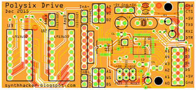
Here's the PCB design that I made using Fritzing.  It's only a two layer board, but it looks awfully complicated for a newbie such as myself.  Does it have any chance of working?

Laying the Groundwork:  Over the last several posts, I've been figuring out most of the elements of this modification, including the digipot and the Arduino.  I know that I want to put all of those elements onto one board and fit it inside my Polysix.  My biggest remaining unknown is how to physically attach my components to the Polysix's circuitry.

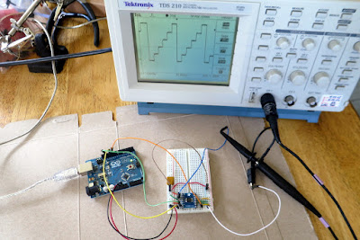
Use One of the Built-In DIP Sockets:  A good trick is to re-use one of the DIP sockets that a used throughout the Polysix circuitry.  This is the same trick that I used when installing my mod to add velocity sensitivity to my Polysix.  For this OTA Overdrive Mod, I'm going to use the DIP socket that the OTA itself lives in (ie, IC20 on the KLM-368 "Effects" PCB).

DIP Socket and DIP Connector:  As shown in the picture below, I'm going to pull IC20 out of its DIP socket and I'm going to insert a pinned DIP-style connector in its place.  My PCB will solder to this pinned connector.  To reconnect IC20 into the circuit, my PCB will include its own DIP socket (and associated wiring).  My PCB will include the wiring to connect IC20 back into the Polysix's circuitry via the pinned connector.

I'm going to attach my PCB via the DIP socket for IC20.  It's great that the Polysix came with so many socketed ICs to enable this kind of hack.

Circuit Block Diagram:  Before diving into PCB design, it's important that I understand what it is that I want to do.  The block diagram below shows my overall approach for this PCB.  It shows the DIP connector and DIP socket, it shows the digipot that controls the overdrive, and it shows the Arduino-style microcontroller that controls the digipot.  It also shows the headers that I'll used to program the Arduino ("ICSP" and "FTDI") as well as a bunch of pins and headers that'll let me be flexible in how I choose to connect the various audio and synth control signals that I might wish to manipulate.

Here's a block diagram of what I'm hoping to build.  I want to include lots of pin headers so that I have plenty of flexibility for modifying my own circuit once it's built.

Which PCB Layout Software?  In my previous attempt at a PCB design, I used CadSoft Eagle This is the PCB layout software common throughout the Maker community, probably because there is a free version that is pretty capable.  Both Sparkfun and Adafruit seem to think that it's a good choice for their open source designs.  I didn't like it, though.  I thought that it was hard to learn and didn't promote self-discovery.  I felt like trying a new tool instead.  I almost went for a cloud-based software tool like Autodesk's 123D Circuits, but at the last moment I ended up downloading and trying Fritzing.  I found Fritzing to be very approachable, and unlike 123D Circuits, it's been around long enough for the forums to have a good number of threads for me to learn from.

To layout my PCB, I tried Fritzing.  It seemed much more approachable than CadSoft Eagle.

Parts then Schematic then PCB:  One should only start a PCB design when you already have a good idea about what you want to build.  That's why I started with the block diagram shown earlier and that's why I spent so much time breadboarding the key elements of my circuit in previous posts.  Once you know what elements are going to be in your circuit, only then should you start with the PCB design software.  PCB design software generally follows a three-step process: (1) choose the parts for your design, (2) draw your schematic using your parts, (3) layout your PCB based on your schematic.  OK, here we go...

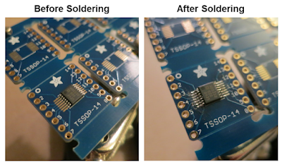
Step 1A: Choosing my Parts. Looking back at my block diagram, my major parts are the LM13600 OTA, the AD5262 dual digipot, and the ATMega 328P microcontroller.  For minor parts, there will be a bunch of resistors and capacitors, some pin headers, and an oscillator/clock for the microcontroller.  Fritzing is already well stocked with parts for me to use for these minor components.  So, it's the major components that I need to focus on.  Lucikly, Fritzing already has the version of the ATMega 328P that I want to use (the surface mount TQFP package).  What Fritzing doesn't have is the LM13600 OTA or the AD5262 digipot.  I needed to make these two parts myself.

Step 1B: Creating the Missing Parts.  Making parts is often the hardest part of using PCB design software.  It's such a pain.  I figured it out through a combination of the Fritzing documentation plus lots of trial and error.  The key to making any progress is that Fritzing already had built-in components of the right size.  They weren't the correct part, but they were the correct size (they already had a TSSOP-16 like my digpot and they already had a DIP-16 like my OTA).  As a result, my task was simply to copy the existing parts and re-name the pins.  Through a combination of the built-in part editor (see screenshot below) and a text editor (to change the labels on the SVG graphics), I was able to create my two parts.  If you're interested, I've shared my Fritzing library on my GitHub here.

One of the hardest part of designing one's own PCB is creating models for the parts that don't come in the standard library. Here, I'm making a model for the AD5262 digipot, which is a TSSOP-16 package.  I also did this for the LM13600 OTA, which is a DIP-16.  This process always seems harder than it should be.

Step 2: Create the Schematic.  With my parts created (go me!), I started creating the schematic.  My final schematic is shown below.  In the upper left, you can see a block corresponding to the DIP connector that'll be used to connect this PCB to the Polysix's KLM-368 PCB.  You can see that most of the pins of the DIP connector get routed down to a DIP socket that I'll put on my board to host the LM13600 OTA chip itself.  You can also see that I've broken out few of the LM13600 pins so that I can manipulate the signals (ie, enable overdrive) with the other parts of my circuit.  The rest of the schematic shows the other elements of my circuit -- in particular, you can see the block for the digipot (bottom left) and the big block for the ATMega 328P microcontroller (center).  The critical connections for the 328P (such as the reset circuit) I copied from the Sparkfun Arduino Pro.  That Sparkfun design is also where I learned the layout for the two programming headers (the FTDI and the ICSP headers).

This is the schematic of all the elements that will go into my PCB.  This defines all the connections between the different circuit elements.

Make it Hackable.  As already mentioned, this design breaks out extra Arduino pins, includes some unconnected "spare pins", and includes a second set of pins for both pots in my digipot.  All of these extra access points are to enable future hacking of my own PCB.  I wanted to include flexibility the design of my PCB so that I can make different connections between the OTA, the digipot, and the Arduino.  Who knows what kind of mods I might dream of in the future?!?  With these extra pins, it'll be easier to have fun explorations.  You've got to be prepared to be spontaneous!

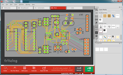
Step 3: Layout the PCB.  With the schematic complete, I started the PCB layout process.  I placed my components onto a notional PCB and started laying wires ("traces") between them.  Below is a screenshot showing all of the parts on a notional PCB outline.  I've got about 2/3rds of the traces complete.  To make a trace you simply choose which side of the PCB you want (top or bottom) and then right-click on one of the "air wires" to create the actual trace.  Because the default trace is pretty thick, I would click on the trace and, in the "Inspector" window pane on the bottom right, choose a thinner size like 12 mil.  Finally, click and drag points on the trace to manually route the trace where you want it.  If a trace needs to jump between layers to avoid existing traces, you create a "via" between the layers by right-clicking on the desired spot on the wire.  This is easy!

This is the PCB layout view in Fritzing.  I'm about 2/3rds complete in laying out the board.
Surface Mount vs Through Hole:  I'm not very experienced with surface mount parts (though I have soldered this TSSOP digipot before), so most of my parts in this design are through hole parts (PTH).  The only two surface mount parts (SMT) are the digipot and the ATMega 328P.  In laying out the PCB, the main issue with mixing PTT and SMT parts is that the grid size (which helps keep your traces orderly) really wants to be different for the PTT components vs the SMT components.  For the PTT parts, grid sizes of 0.1", 0.05" or 0.025" all work well.  By contrast, the TQFP package for the ATMega 328P works better with a 0.8 mm (0.0315") grid.  Annoyingly, for the TSSOP package for the digipot, the best grid size is yet a different value (0.0254").  It gets very tedious manually switching between the different grid sizes.

Finishing the PCB:  Once I got all the traces where I wanted them, I started adding text to the PCB so that I could know where to connect my different signals.  I also put a name and date on the board so that I could know which iteration of he board I was using (surely, I would need to iterate the board to fix errors).  Finally, on the bottom layer, I told Fritzing to do a "copper fill".  This is a common technique to try to reduce unwanted noise that may be transmitted between closely spaced circuit boards (such between this PCB and the Polysix KLM-368 that'll be right underneath it).  A screenshot with my final PCB is shown below.  I shared my Fritzing design files on GitHub here.

Still in Fritzing, I have finished my PCB design, including a big copper fill on the bottom for the ground plane.

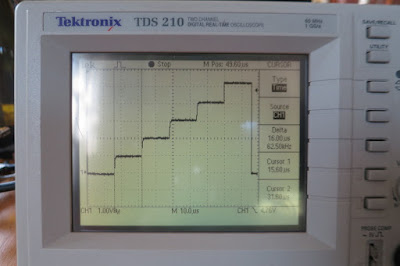
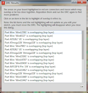
Design Rule Check:  Throughout the PCB layout process, I would periodically use the software's built-in tool for confirming that my traces were not overlapping with anything else on the board.  The traces on a PCB can get pretty convoluted, so using an automated tool is a great benefit.  This tool is called the "design rule check" (DRC) and is included with almost any PCB design software.  In Fritzing, when I'd run the DRC, I'd get a big pile of error messages like shown in the window below.

The "design rule check" (DRC) gives lots of errors for my design when using the default DRC rules.

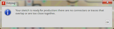
Shrinking the Keepout Distance:  When I would try to find these errors in my PCB, I often saw no issue.  The traces (especially around the SMT components) may have been close, but they were not interfering.  I was confused.  The answer is that the default rules used by the DRC algorithm were too tight for my small SMT components.  When I changed the DRC "keepout" distance from its default 0.01" value to a smaller 0.008" value (see screenshot below), almost all of my errors went away.  The remaining DRC errors were legitimate problems, which I found and fixed.

With such small SMT components, you need to reduce the "keepout", thereby telling the DRC algorithms that it is OK if the traces are close together.  I dropped the keepout from 0.01 inches to 0.008 inches.

Shrinking the keepout (plus fixing some actual errors in my PCB) eventually lets me pass the DRC.

Export for Production:  Once my design was complete and the DRC results came back clean (see screenshot above...I was so happy when I saw this message!), it's time to export the design so that it can be sent out to be printed.  The exported production files are often called "Gerber Files".  In Fritzing, I chose to export to "Extended Gerber Files".  It created a collection of files that define the top and bottom copper traces, the drill locations for the vias and the PTT components, the top and bottom solder mask, and the top and bottom silkscreen (ie, text and graphics).  These are the files that the printing company need to make the PCB.

Tailor for Your PCB Print Company:  Unfortunately, every PCB printing company is a little different in their requirements for the Gerber files.  As a result, the Gerbers may have to be tweaked specifically for different printing companies.  For me, I chose to use OSH Park to print my board.  Looking at their requirements, the Fritzing Gerber files were all fine, except I had to change my drill file to end with ".xln".  That's all I had to do!  My Gerber files are zipped up on my GitHub here.

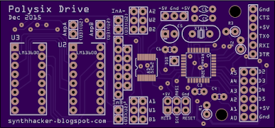
Send to Printer:  I uploaded my zipped Gerber files to OSH Park.  Their automated system interprets the files and then shows you illustrations of your design so that you can confirm that they interpreted your files correctly.  In my case, the top and bottom views of my board are shown below.  They look pretty good.


Top and Bottom View of my PCB as Generated by OSH Park.  $21.75 for three.  Let's get it printed!

Order the PCB:  In general, the cost for PCBs is driven by the number of layers (a two-layer board is cheaper than a six-layer board) and by the area of the board (a smaller board is cheaper than a large board).  I tried to make my board pretty small.  I was hoping to get under $20, but I only got it down to $21.75.  Given that OSH Park sends you three copies of your board for that price (plus free shipping!), I'm still pretty happy.  Anyone can order my board from OSH Park here.

Waiting:  So, now I wait for the board to get printed and sent to me.  It generally takes 2-3 weeks.  I'm so excited to get it.  Waiting is agony!

Replacing Key Contacts on Korg Mono/Poly

$
0
0
When I first got my Korg Mono/Poly off eBay, quite a few of the keys didn't play.  After some searching around, I tried some CaiKote on the rubber key contacts (as I described here) and it worked great.  When I bought a Korg Polysix off eBay, it had the same problem...and CaiKote saved the day again.  But, now that it's been a few years, some of the keys on the Mono/Poly have stopped working again.  Let's fix this problem for-real.  Let's replace the key contacts!

New Key Contacts from LA Synth Co

When I first had my problem with dead keys, I couldn't find anyone who sold new key contacts for these old synths.  So, I had to use the CaiKote to restore the old ones.  That was pretty cheap and pretty easy.  I now know, however, that it's a fix that only lasts a few years.  In that time, LA Synth Co has started to sell brand new key contacts that fit a bunch of old synths from that era.  Fantastic!  So, $100 later, I've got a complete set to fit my Mono/Poly.  Let's take the old girl apart and swap in these new parts!

First, remove the five screws on the bottom of the synth to release the keybed.  Then, remove the screws holding on the metal panel so that you can get inside.  Finally, unplug the keybed from the Mono/Poly circuitry

Getting started is pretty easy.  As shown above, I unscrewed the keybed and the main front panel.  Then, I opened up the synth and disconnected the keybed from the circuitry.  At that point, I was able to pull out the keybed.

The keybed has been removed from the Mono/Poly.

With the keybed out of the synth, you can look at the side of the keybed and see how, when pressing a key, the key smashes down a gray rubber button (the "key contact") onto the circuit board underneath.  It is through this contact that the brains of the synth know that the human has pressed a key.

You can see how pressing a key acts to press down the gray rubber key contact.

On the underside of the keybed, you can see the brown circuit board.  The key contacts are attached to this board.  We need to remove this board to get access to the key contacts.

The underside of the keybed has a brown circuit board.  Remove the screws to release the board.

Removing the screws, the brown circuit board is easily removed.  Flipping it over, you can see all of the gray rubber key contacts.  They come off simply by tugging on them.

Removing the circuit board, the gray key contacts are revealed.

Pulling on the gray rubber strips, the key contacts are easily removed.

With the old key contact strips removed, now was a good opportunity to get out a little alcohol and clean the contacts on the circuit board.  I probably should have used higher quality alcohol (only 70%?), or something better than a cotton rag for my scrubber, but this is what I had.

Time to clean the circuit board.

With the board cleaned, I got out the new key contacts and lined them up to make sure that I had the correct assortment -- they're not all the same and I was worried that I might not have been sent the right ones.  Luckily, LA Synth Co know what they are doing.  I had what I needed.  They lined up great and I attached them simply by pushing them on.

Getting ready to attach the new key contacts
The new key contacts are attached simply by pushing them on.

With the key contacts attached, I start putting the synth back together again.  First, I have to re-attach the key contact circuit board to the bottom of the keybed.  The only trick is getting the key contacts to fit inside their respective holes in the bottom of the keybed.  It isn't hard, but you do have to pay attention.

These are the holes on the bottom of the keybed into which the key contacts must fit. 

After getting the board onto the keybed and screwed together, I did a visual inspection and saw that one key contact wasn't seated correctly (as shown below).  So, I unscrewed the board and was more careful in putting them together.  The second time, all the key contacts were seated nicely.

Here, after assembly, one of the key contacts didn't seat correctly.  I simply took it apart and was more careful when I put it together again.

That's it!  The key contacts are done!  The only thing left to do is to put the synth back together again.  I have to put the keybed back in, screw it in, and screw the front panel back down.

Time to put everything back together again!

Fully re-assembled, I also to this as an opportunity to clean the keys and the front surface.  Looks great!

The re-assembly went easily.  I also used my rag and alcohol to clean the tops of the keys and the control panel.  She looks great now!

Plugging her in, they keys all work.  The joy!  Not only is it a joy to play an instrument that works, it's a real satisfaction to have fixed it myself.  Fixes don't really come any easier than this one.  Thanks LA Synth Co!

DIY MIDI Ribbon Controller

$
0
0
In a previous age of the world (2011), I built myself a ribbon controller.  I used it to drive my Korg Mono/Poly via CV.  And it was good.  But, that was before "synthhacker" first awoke under the stars on the shores of Cuivienen.  Has its glory been forever lost?  No!  The ribbon lives again!  And it has been updated!  Behold:


The Overall Setup:  This ribbon is just a controller -- it controls a synthesizer.  It doesn't make noise itself.  Those black-and-white keys that are built into the synthesizer are also just a controller.  They tell the brain of the synth to make noise at fixed pitches.  My ribbon controller uses the synth's MIDI interface to tell the synth to make noise across a continuous spectrum of pitches.  More bendy.  More swoopy.  Fun!  My controller has two parts: the ribbon itself, and some electronics (Arduino +  MIDI Shield) to do the ribbon-to-MIDI conversion.


The Ribbon Parts:  The ribbon itself, I built a long time ago.  But, as stores on the internet never forget what you've ordered, I easily went back and looked it up.  The core of the ribbon controller is a 500mm-long "soft pot" (Sparkfun).  This is the part that senses where you touch.  Since it is soft and floppy, however, I also bought a 2-ft long strip of plastic (McMaster) to act as a backbone.  For the electrical connection to the ribbon, I used a headphone jack (Sparkfun) and a small perfboard (Sparkfun).  The only real innovation with my ribbon controller (there are lots of DIY ribbons out there) is that I also added a magnetic strip along its back (McMaster).  Since most of my synths  have a metal front panel, the magnetic strip is a great way of keeping the ribbon in place!

Components of the Ribbon Controller

The soft pot is on the top.  The magnetic strip (partly unrolled) is in my hand.

Assembling the Ribbon:  I started with the plastic strip.  Its edges were surprisingly shart, so I got out some sandpaper to smooth the edges.  Now it's much nicer to touch.  After cleaning off the sandy bits, I spray-painted the whole thing black.  When fully dry, I attached the magnetic strip and the soft pot, both via their adhesive backing.  Then, I carefully soldered the ribbon's terminals (don't melt the soft pot!) to the perfboard and then to the audio connector.  I wired the connector so that the "top" of the pot was to the tip, "bottom" of the pot was to the sleeve, and the "wiper" of the pot was to the ring.  Once it was all soldered together, I epoxied the perfboard to the plastic strip to make it all nice and solid.

Headphone jack is connected to the perfboard, which is connected to the soft pot.  The whole thing is epoxied to the plastic strip, for strength.

Arduino-MIDI Electronics:  The ribbon is just a potentiometer -- it needs electronics to interface to a MIDI synth.  After my previous project making an MIDI-to-trigger converter, I realized that I could re-use that exact same hardware for this ribbon-to-MIDI converter.  Repeating the recipe list from that project, my parts include an Arduino Uno, a MIDI Shield* from Sparkfun, some stackable headers, and a 3.5 mm stereo headphone jack (or maybe one like this).

(* Note: I used the old Sparkfun MIDI Shield but, presumably, the new model linked above works well, too).

Components for the "Brain" of the Ribbon Controller

Assembling the Electronics:  I soldered together the MIDI shield, including soldering on the stackable headers.  I then soldered some wires to the audio jack and soldered those wires (being sneaky) to the header pins sticking down from the MIDI shield (detailed soldering pics here).  Once it was all assembled, I connected the ribbon to the MIDI shield using a standard 3.5 mm audio cable.  I also connected a USB cable to my laptop so that I could power it and program it.  The photo below also shows the MIDI cable connected, but we're not quite ready for that, yet.

Connecting my ribbon controller to the MIDI Shield (the Arduino is under the MIDI shield).

The Ribbon is a Potentiometer:  Touching the ribbon (the "soft pot") is like turning the knob on a potentiometer to a particular spot.  If I touch it near the low end, it'll show a low resistance.  If I touch it near the high end, it'll have a high resistance.  The job of the Arduino, therefore, is to sense the resistance of the ribbon so that it knows what note to play.  In theory, pretty easy.  But, to get some details on how this works, I hooked used my setup to collect some actual data.

The Ribbon's Response via Arduino:  To measure the response of the ribbon with an Arduino, I used the setup described above, which has the wiper of the pot connected to one of the Arduino's analog input pins (A3).  The bottom of the pot is tied to ground.  I activated the input pin's pullup resistor (via pinMode(A3, INPUT_PULLUP)) and started reading ribbon values via AnalogRead(A3).  I printed the values to the serial port so that I could see them on the P and log them to a file.  Sliding my finger to different octave points on the ribbon, I made the plot below,

The AnalogRead() Values Generated by the Arduino when Touching the Ribbon at Different Spots.

Values When Not Touching the Ribbon:  The first thing to notice is what happens when *not* touching the ribbon: the ribbon shows a very high value.  The high value results from the fact that the wiper is floating when you're not touching the ribbon.  As a result, the pull-up resistor on the analog input pin is able to pull the value all the way to the maximum value (which is 1023 on the Arduino Uno).  So, it's easy to know when you're touching the ribbon versus non touching the ribbon -- just look to see if the value is near 1023.

Values When Touching the Ribbon:  The middle of the graph shows the values when I touch the ribbon between its bottom (C1) and its top (C4), Looking at the detailed values, the lowest value seen in my ribbon (C1) is about 12 whereas the highest value (C4) is about 339.  So, I know that I have to program the Arduino to map values between 13-339 to musical notes between C1-C4.

Touching the Ribbon To Record the Arduino's AnalogRead() Value at Different Locations.

Software:  After seeing how the ribbon responds, I wrote my Arduino software.  It's basically a big loop that reads the ribbon value, converts it to a MIDI note number, and sends those MIDI commands to my synth.  While it seems conceptually simple to do an AnalogRead() for the ribbon followed by a Serial.write() to send the corresponding MIDI message, it does actually take some thought to get it to respond the way that you'd like.  Also, to make the ribbon pitches change continuously (and not be quantized like with the piano keys), you need to compute and transmit all the pitch bend commands.  It takes some work to get it right.  If you're interested, my Arduino code is available on my GitHub here.

Linearizing the Response:  One tricky spot is if you want the pitch to track linearly with your finger position on the ribbon.  In my case, I found that the notes were too closely-spaced at the top of the ribbon and too widely-spaced at the bottom.  I didn't like that.  The key to linearizing the response is to recognize that the ribbon and the Arduino's pull-up resistor actually form a voltage divider.  Once you do the math on that voltage divider, you program the Arduino to better deduce the note you want given the apparent voltage at the soft pot's wiper.  It's not perfect, but it's much better than before.

I was lucky at how well the ribbon fits on the face of the synth.  I took the extra effort to make the software fit well, too.
Bend Range:  The ribbon is fun because you can use your finger to sweep through all the pitches in between the normal notes.  Since the MIDI messages assume a piano-like keyboard, you do these "in between" pitches by commanding a note to one of the standard pitches followed by commanding a pitch bend to get the in-between pitch that you actually want.  Ideally, you could set the synth so that its allowable amount of bend would span the whole ribbon.  Unfortunately, on the Prophet 6, the max bend amount is +/- 1 octave.  As a result, with my setup, I get a brief note discontinuity when I try to continuously slide across more than 1 octave.  This is a limitation of the synth, not my ribbon controller. (If the synth's software were open source, I could fix that!)

Wobbling Pitch (ie, Pitch "Noise"):  Another subtlety that I uncovered is related to the fact that one's ear is very sensitive to changes in pitch.  The issue is that any noise in the measurement of the ribbon value will directly translate into wobble (instability) in the pitch commands sent to the synth.  When I was powering my system from the laptop and when the laptop was running on battery, my system sounded great.  But, when I plugged the computer into AC power, the pitch wobbled a lot.  It was quite unpleasant.  My solution was to add a 33 nF capacitor between the ribbon's analog input pin and ground and to add some filtering in software (revised code is here).

Future Work:  It's pretty fun to have my ribbon controller working with my MIDI synth.  Sure, I don't like that there is still a note discontinuity that happens when I try to exceed the 12-step max bend allowed by the Prophet 6, but it's still quite fun.  (Maybe I can sweet talk someone at Dave Smith Instruments to help me out on that one remaining issue :).  Looking for other ways to improve the ribbon, I'm considering adding a DAC so that the the Arduino (or Teensy!) can directly create its own audio without needing to command an external synthesizer.  That'd be fun.  How about a ribbon wavetable synth!  Or, how about a ribbon FM synth?  Fun!

DIY Ribbon Controller - CV

$
0
0
In sharing my work on a MIDI-enabled ribbon controller, a couple of the good folks at Muff Wiggler wanted more.  They wanted to see a CV-enabled ribbon.  So, as I'm always ready for more hacking, today I present for your enjoyment: my home-brew CV ribbon controller.


Switching from MIDI to CV:  This CV-enabled ribbon builds directly upon my MIDI ribbon.  It uses literally the same ribbon, which I built (like everyone) using a $20 soft-pot sensor.  Like my MIDI ribbon, This CV ribbon also uses an Arduino to sense ribbon and to generate the commands for the synth.  The main thing that is different with the CV ribbon is that I needed to add a digital-to-analog converter (DAC) to generate the CV signals that'll drive my old synths.

The only difference between the MIDI ribbon and the CV ribbon is how the Arduino outputs its commands.  The MIDI ribbon uses an Arduino "MIDI Shield" to send the MIDI messages whereas the CV Ribbon uses a DAC to generate the CV voltages.

Using a DAC:  A DAC is a device for generating arbitrary analog voltage signals.  You send it commands (such from an Arduino) and its output jumps to the voltage level that you desire.  They're very handy devices for synth hacking.  My experience is with the MCP4922, which is a 2-output, 12-bit DAC.  After refreshing my memory using its datasheet, I decided to wire the DAC to the Arduino as shown in the schematic.

The ribbon (left)  is wired to the Arduino (left-center).  The Arduino is wired to the DAC (right-center).  The DAC is wired to the CV outputs (right).  Easy.

Wiring the DAC:  From this schematic, I used a solderless breadboard to wire up my DAC.  I chose to use an Arduino Micro because it easily fits into the breadboard (unlike an Arduino Uno).  Wiriting software for the Micro is the same as for the Uno, so it's a trivial swap.  The wiring diagram below (go Fritzing!) shows my plan for wiring the DAC to the Arduino.  I added the headphone jacks to make it easy to get the signal in from the ribbon and to get the CV signals out to the synth.  For breadboarding, I like using this jack with this breakout from Sparkfun.

My wiring plan for the Arduino Micro and the MCP4922 DAC.  Power is supplied from USB connection to the Arduino.

Real-World Wiring:  Of course, once real wires are involved, it never looks as pretty as the plan.  The picture below shows my actual breadboard with its actual wires.  All the connections are the same, but the routing is different.  Also, I moved where I put the headphone jacks: the ribbon input is the one on the bottom right and the two output jacks are dangling off the back (one is black, the other beige).  Note my use of the blue rubber band to keep the output jacks somewhat contained.

The real-world wiring is never as nice as the plan.

Pitch and Trigger CV Signals:  For this hack, I'm generating three signals to control my synth: a pitch CV, a trigger (a.k.a. gate) signal, and a filter CV.  The pitch CV controls the pitch of the synth.  It's a signal that can take any value between zero volts (a low pitched signal) and 5V (a high pitched signal).  The trigger signal, by contrast, is simply low (0V) or high (5V).  It tells the synth whether the note is "on" or "off".  Since it is just a LOW/HIGH signal, it is generated by one of the Arduino's digital pins, not the DAC.

Filter CV:  The last signal that the system generates -- the filter CV -- controls the cutoff frequency of the filter.  Like the pitch CV, it can be any value between 0-5V, and so I use the 2nd channel of the DAC to generate it.  I added this capability to the system (like I did with the MIDI version) so that the filter opens up a bit as you play higher notes.  This is the same kind of interaction you'd get with the keyboard if you had the "keyboard tracking" turned up about half-way.  Adding this behavior made the ribbon feel more natural and more engaging.

In response to the ribbon, the Arduino+DAC generates three signals: pitch CV, trigger CV, and filter. CV 

Arduino Software:  With the hardware assembled, and with my CV signals decided, I wrote the software for the Arduino.  I reused my software for the MIDI ribbon and simply added the functions to drive the MCP4922 DAC.  My code is available on my GitHub here.  Having both the MIDI and CV functionality in one program makes it more complicated to read, but it gets the job done.

The Korg Mono/Poly has good flexibility for interfacing to external gear.  Here, my circuit is creating CV signals that I'm injecting to control the filter cutoff ("VCF fcM IN", on the left), to control the gating of the note ("TRIG IN"), and to control the pitch of the note ("CV IN").

Putting it All Together:  With the software written, and with the CV signals injected into the correct locations on the back of the synth (see pic above), I was ready to get to the business of playing.  Of course, it didn't work the first time,but after some debugging (should the Trigger signal be set high or low on the Mono/Poly?), I got it to work pretty well.  Interestingly, I found myself playing the ribbon differently when attached to my Mono/Poly than when it was connected to my Prophet 6.  I think that it had something to do with the CV vs MIDI.  MIDI is designed for discrete pitch instruments (like keyboards).  I feel that the continuous pitch of a ribbon is just better suited to CV.

My old Mono/Poly, with the magnet-backed ribbon just above the keybed, and with my magnet-backed breadboard controller in the upper-left.

Next Steps:  Now that I have a DAC working, it opens all sorts of possibilities.  A DAC could be used to generate audio signals directly, not just CV signals.  By directly synthesizing its own audio, I could make the ribbon a stand-alone instrument.  Yes, using these electronics to create a wavetable ribbon synth could very, very interesting.

DIY MIDI Breath Controller

$
0
0
Breath controllers are a difficult subject to bring up.  They have a bit of a bad reputation...perhaps because of synthesized saxophone sounds.  Breath controllers often induce people to roll their eyes dismissively.  It's kinda like how many people respond to keytars.  Are they awesome?  Or are they cheesy?  How can you know, if you've never played one?  Well, a buddy of mine started sending me links about DIY breath controllers (see Mixtela's MK1 and MK2).  He knows I'm a sucker for DIY.  So, with this as motiviation, I pulled together my own plan and made my own DIY MIDI breath controller.


Breath Controller?  The idea of a breath controller is that you use your pressure from your breath to control some aspect of your synthesizer.  The harder you blow, you make your synth louder, or you open its filter more, or you bend its pitch.  Some breath controllers are shaped like wind instruments and include both breath sensitivity and buttons (keys) to change notes.  Other breath controllers (such as mine) are simpler and just have the breath-sensitive part.  With only the breath-sensitive part, you control sound parameters on our synth, like having a breath-controlled mod wheel.

My Approach.  I'm choosing to have my breath controller use MIDI messages to control my synth.  Therefore, I'll need to (1) choose a pressure sensor, (2) connect it to some sort of electronics to read the signal, and (3) write some software to send MIDI messages to my synth.  Let's do it!


The Shopping List.   First, let's go shopping.  There are lots of ways to build this device.  Below are the components that I used:

  • Pressure Sensor: Honeywell NSCDRRN0001NDUNV.  This is a differential pressure sensor whose output voltage changes as pressure (positive or negative!) is applied.  The pressure range of this sensor is +/- 1 inch of water (about +/- 250 Pa).  It can be bought it from Mouser, but it's not cheap.  Cheaper sensors will probably work, too. 
  • Flexible Tubing: I used Tygon clear tubing.  To fit onto the sensor's snout, you need a short length of 1/16" ID tubing (here), but most of your length should be 1/8" ID (here).  You want that larger diameter so that you can push enough air through it to be comfortable.  Bigger tubing might be even better.
  • Electronics:  I used an Arduino Uno because I had one around.  You can probably use any hobbyist microcontroller board (including the Redboard or Metro) but you want one that'll mate to your MIDI Interface.
  • MIDI Interface:  I used the Sparkfun MIDI Shield.  I like that it has built-in pots so that I can adjust things while playing.  Note that it does not come with the header pins, so be sure to buy some...you should definitely buy stackable headers.
  • Prototyping Supplies:  I did my prototyping on a solderless breadboard.  I also used some little jumper wires that are typical in the Arduino world.   
  • Power:  During development, I powered the system from my computer's USB port.  But, when I was done, I wanted to be free from the computer.  So, I've been using USB power wall-wart like this one along with a standard USB cable.

Wiring It Up.  After assembling the MIDI shield and plugging it on top of the Arduino, I needed to figure out how to wire up the pressure sensor. After digging through the datasheet for the pressure sensor, I found the information I needed (copied it below).  It has three types of connections: power pin, ground pin, and two output voltage pins (and you can ignore one of them, if you want).  Easy.


Using the solderless breadboard and my jumper wires, I connected the sensor to the Arduino via the MIDI Shield's stackable headers:
  • Sensor Pin 1 to Arduino 5V
  • Sensor Pin 2 to Arduino analog input A2
  • Sensor Pin 3 to Arduino analog input A3
  • Sensor Pin 4 to Arduino ground
After adding the flexible tubing to the snout of the pressure sensor, the hardware is ready.


Arduino Software.  Once it is assembled, you need to write a software to command the Arduino to read the sensor and to issue MIDI commands.  There are lots of choices here, but at it's core, it is three steps:
  • An "analogRead" to measure the output of the pressure sensor
  • Arithmetic to convert the measurment to a valid MIDI value (usually 0-127)
  • A few "Serial.write" commands to send the MIDI message to the synth
In practice, things are modestly more complicated.  Really, though, the primary question is what MIDI message you want to send.  Everything depends upon that. 

Choose Your MIDI Command!  There are many ways to command your synth via MIDI.  You need to find out what MIDI commands your synth can respond to and what is easy for you to configure (three good choices are shown below).  On my synth, aftertouch is very easy to set up without any menu diving.  So, I chose to have my breath controller send aftertouch MIDI messages.  Later, I made it more complicated, but aftertouch is still what I use most of the time.  My code is available on my GitHub here.

From midi.org
Initial Disappointment.  Once I got my system working, I had to learn how to play a breath controller with my synth.  I quickly become bored because all I could make it do were relative slow filter sweeps or unusable pitch bends.  There was no way to give it articulation because it was simply about lung pressure...and my chest does not have much dexterity for quick motions.  Disappointment.

The Key is Airflow.  After some messing around, I had the idea to poke a hole in my tubing so that some air could flow through the tube and out the hole.  Once I did that, everything changed.  I quickly found that I could use very quick motions like tongue-stops on the tip of the tube (in my mouth).  Suddenly, it could respond quickly, like any other wind instrument.  Without the hole, tongue-stops had no effect because the sealed tube kept the pressure high.  With the hole, however, the air vents out when the tongue stops its end.  Therefore, the sensor sees a quick change in pressure and articulation is achieved.  It's so much more varied and expressive this way.  The vent hole in the tube is the key.

It's Fun.  With this modification, I found myself having fun with the breath controller.  Yes, I could still do slow swells on sustained pads.  But, now I could also articulate fast riffs, giving them a new kind of bounce.  Using the breath controller on repetitive arps, I could literally "breathe" life into them via breath-modulating the filter.  And, for single note work, the breath controller is great for contouring one's phrases in a way that is very difficult to do any other way.  So, while I wouldn't use a breath controller in every situation, it is a good time.  I recommend trying it.  And maybe even making it yourself!
Viewing all 82 articles
Browse latest View live